Researchers detail DarkTortilla, an evasive crypter used by hackers to spread a broad array of commodity malware and targeted payloads.


Jupiter’s icy moon Europa is an ocean world encased beneath a thick crust of ice — a place where snow floats upward.
The underwater snow forms in the global ocean and travels up though the water to attach to submerged ravines and inverted ice peaks, according to new research. This same phenomenon takes place below ice shelves on Earth — and it may be how Europa builds its ice shell.
The finding, published Monday in the journal Astrobiology, suggested Europa’s ice shell may not be as salty as scientists first thought. Understanding the salt content of the ice crust is crucial as engineers work on assembling NASA’s Europa Clipper spacecraft, which is preparing to launch to Europa in October 2024.


For general readers:
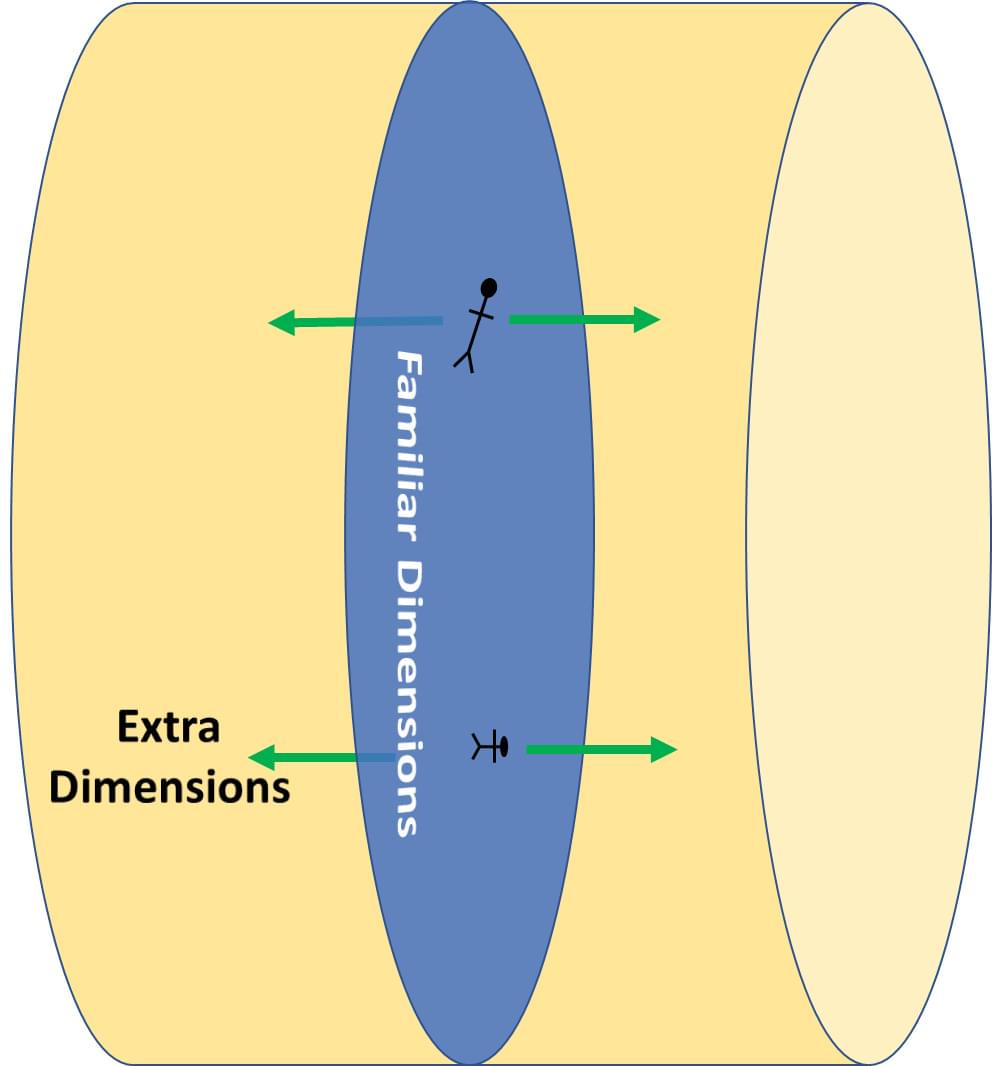
Is it possible that the particle physicists hard at work near Geneva, Switzerland, at the laboratory known as CERN that hosts the Large Hadron Collider, have opened a doorway or a tunnel, to, say, another dimension? Could they be accessing a far-off planet orbiting two stars in a distant galaxy populated by Jedi knights? Perhaps they have opened the doors of Europe to a fiery domain full of demons, or worse still, to central Texas in summer?
Mortals and Portals.

Cells use selective autophagy or self-degradation of undesired proteins to maintain cellular homeostasis (i.e., a state of balance). This process is controlled by autophagy receptors, which mediate the selection of a target protein that is subsequently “cleared.”
Tau proteins, which play a crucial role in the internal architecture of neurons in the brain, abnormally accumulate within neurons in disorders such as dementia and Alzheimer’s.
Alzheimer’s disease is a disease that attacks the brain, causing a decline in mental ability that worsens over time. It is the most common form of dementia and accounts for 60 to 80 percent of dementia cases. There is no current cure for Alzheimer’s disease, but there are medications that can help ease the symptoms.
Famed researcher Dr Aubrey de Grey speaks with Martin O’Dea, CEO of Longevity Events, ahead of the inaugural Longevity Summit at Dublin’s Mansion House next month. The Round Room on Dublin’s Dawson Street will host some of the world’s renowned longevity experts including Aubrey de Grey, Co-Founder of SENS Research Foundation.
de Grey is really looking forward to this 3-day event in September 2022 to network, educate, research, meet and nurture the global longevity relationships through meeting unique individuals, companies, foundations and investors from all corners of the globe.

You don’t have to know a whole lot about science to know that black holes normally suck things in, not spew things out. But NASA detected something mighty bizarre at the supermassive black hole Markarian 335. Two of NASA’s space telescopes, including the Nuclear Spectroscopic Telescope Array (NuSTAR), amazingly observed a black hole’s corona “launched” away from the supermassive black hole.
Then an enormous pulse of X-ray energy spewed out. This kind of phenomena has never been observed before.
Computer chip designers, materials scientists, biologists and other scientists now have an unprecedented level of access to the world of nanoscale materials thanks to 3D visualization software that connects directly to an electron microscope, enabling researchers to see and manipulate 3D visualizations of nanomaterials in real time.
Developed by a University of Michigan-led team of engineers and software developers, the capabilities are included in a new beta version of tomviz, an open-source 3D data visualization tool that’s already used by tens of thousands of researchers. The new version reinvents the visualization process, making it possible to go from microscope samples to 3D visualizations in minutes instead of days.
In addition to generating results more quickly, the new capabilities enable researchers to see and manipulate 3D visualizations during an ongoing experiment. That could dramatically speed research in fields like microprocessors, electric vehicle batteries, lightweight materials and many others.

