Scientists in China have performed an experiment first proposed by Albert Einstein almost a century ago when he sought to disprove the quantum mechanical principle of complementarity put forth by Niels Bohr and his school of physicists. Bohr claimed there are properties of particles that cannot simultaneously be measured. The new result backs up the Copenhagen school yet again, with the potential to shed light on other, less settled questions in quantum mechanics.
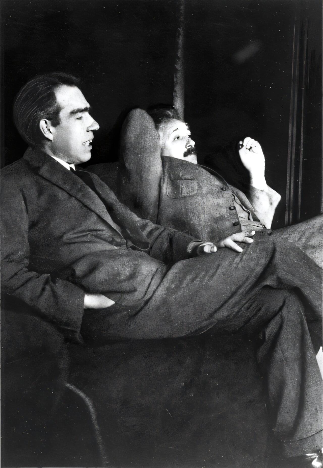
When they met at physics conferences, Albert Einstein and Niels Bohr liked to kick back and debate about quantum mechanics. Einstein, always skeptical of the standard picture of quantum mechanics then being developed, liked to claim he had found holes and inconsistencies in Bohr’s interpretation, and Bohr was always up for the challenge.
At the 1927 Solvay conference in Brussels, the two Nobel Laureates had perhaps their most famous parley, with Einstein famously proclaiming, “God does not play dice with the universe.” In particular, Einstein proposed an experiment he thought would reveal the essential contradiction in the principle of complementarity, which held that pairs of properties of particles, such as position and momentum, and frequency and lifetime, cannot be measured at the same time. Complementarity undergirds the concepts of wave-particle duality and Heisenberg’s uncertainty principle.