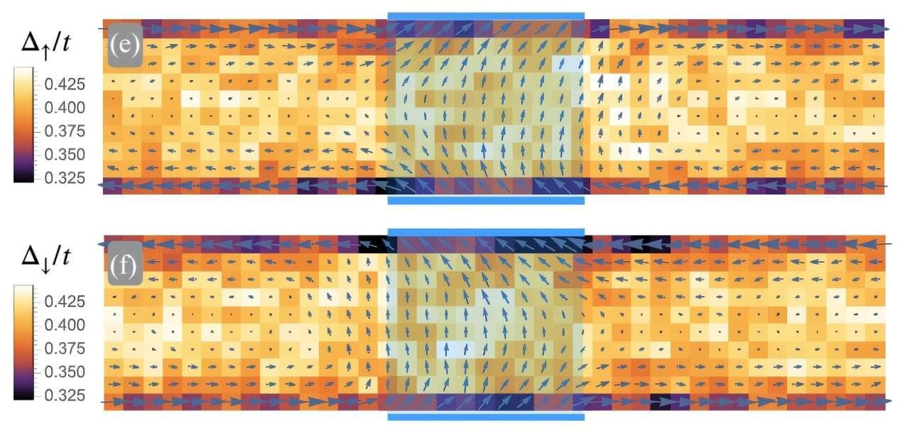
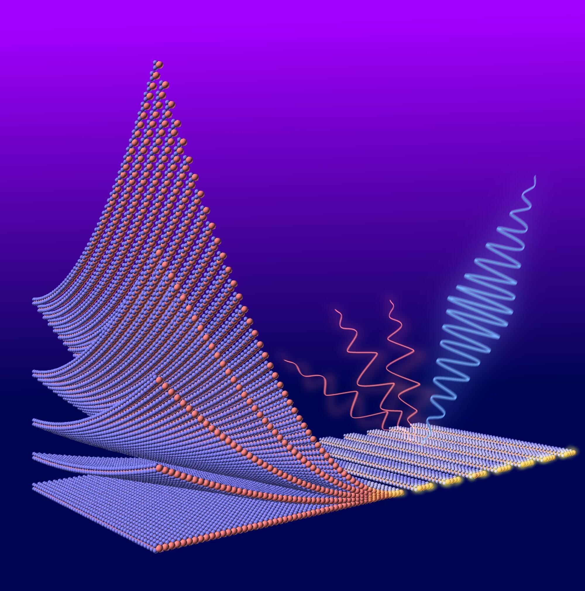
Researchers have proposed that a newly identified class of magnetic materials could extend the zero-resistance currents of superconductors to electron spins. Publishing their calculations in Physical Review X, Kyle Monkman and colleagues at the University of British Columbia propose how “altermagnets” could enable persistent spin currents to flow without dissipation. If confirmed experimentally, the effect could provide a powerful new platform for spintronics, where information is encoded in spin rather than electric charge.
The ability to transport spins over long distances is a central challenge in spintronics. In conventional metals and semiconductors, spin currents decay rapidly due to effects that randomize electron spins. One promising workaround has been superconducting spintronics, where dissipationless charge transport is combined with magnetic materials. However, these hybrid systems often suffer from intrinsic drawbacks, including stray magnetic fields that can interfere with nearby components, suppressing superconductivity.
First confirmed in 2024, altermagnets offer a potential way around these problems. Like antiferromagnets (where a magnetic dipole’s spin is always opposite to those of its neighbors), they have zero net magnetization, avoiding unwanted magnetic fields.
