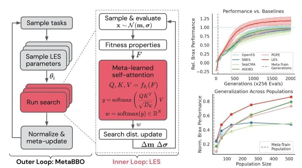
Black box optimization methods are used in every domain, from Artificial Intelligence and Machine Learning to engineering and finance. These methods are used to optimize functions when an algebraic model is absent. Black box optimization looks into the design and analysis of algorithms for those problem statements where the structure of the objective function or the limitations defining the set is not known or explainable. Given a set of input parameters, black box optimization methods are designed to evaluate the optimal value of a function. This is done by iteratively assessing the function at multiple points in the input space so as to find the point that generates the optimal output.
Though gradient descent is the most used optimization approach for deep learning models, it is unsuitable for every problem. In cases where gradients cannot be calculated directly or where an objective function’s accurate analytical form is unknown, other approaches like Evolution Strategies (ES) are used. Evolution strategies come from evolutionary algorithms, which refer to a division of population-based optimization algorithms inspired by natural selection. Basically, Evolution Strategies (ES) is a type of Black Box Optimization method that operates by refining a sampling distribution based on the fitness of candidates and updating rules based on equations.
In a new AI paper, researchers from Deepmind, have introduced and developed a new way to use machine learning to learn the update rules from data, called meta-black-box optimization (MetaBBO), to make ES more flexible, adaptable, and scalable. MetaBBO works by meta-learning a neural network parametrization of a BBO update rule. The researchers have used MetaBBO to discover a new type of ES called learned evolution strategy (LES). The learned evolution strategy LES is a type of Set Transformer that updates its solutions based on the fitness of candidates and not depending upon the ordering of candidate solutions within the Black box evaluations. After meta-training, the LES can learn to choose the best-performing solution or update solutions based on a moving average.


