Toggle light / dark theme

UV tattoos use a fluorescent dye, which means the tattoo only appears under UV light. There is little evidence on whether UV tattoos are safe for human skin.

UV tattoos, also known as black light tattoos, are invisible under regular lighting and only appear under UV light due to the fluorescent compounds within the ink.

There is no regulation over UV tattoos, so there may be some potential health risks, depending on the ink’s chemicals. UV tattoos will also require similar aftercare to regular tattoos.

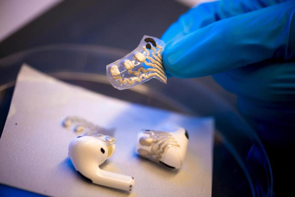
The field of epidermal electronics, or e-tattoos, covers a wide range of flexible and stretchable monitoring gadgets that are wearable directly on the skin. We have covered this area in multiple Nanowerk Spotlights, for instance stick-on epidermal electronics tattoo to measure UV exposure or tattoo-type biosensors based on graphene; and we also have posted a primer on electronic skin.

Taking the concept of e-tattoos a step further, integrating them with triboelectric nanogenerators (TENGs), for instance for health monitoring, could lead to next generation wearable nanogenerators and Internet-of-things devices worn directly on and powered by the skin.

In work reported in Advanced Functional Materials (“Triboelectric Nanogenerator Tattoos Enabled by Epidermal Electronic Technologies”), researchers report a tattoo-like TENG (TL-TENG) design with a thickness of tens of micrometers, that can interface with skin without additional adhesive layers, and be used for energy harvesting from daily activities.

Year 2019 😁


Semiconducting carbon nanotubes (CNTs) printed into thin films offer high electrical performance, significant mechanical stability, and compatibility with low-temperature processing. Yet, the implementation of low-temperature printed devices, such as CNT thin-film transistors (CNT-TFTs), has been hindered by relatively high process temperature requirements imposed by other device layers—dielectrics and contacts. In this work, we overcome temperature constraints and demonstrate 1D–2D thin-film transistors (1D–2D TFTs) in a low-temperature (maximum exposure ≤80 °C) full print-in-place process (i.e., no substrate removal from printer throughout the entire process) using an aerosol jet printer. Semiconducting 1D CNT channels are used with a 2D hexagonal boron nitride (h-BN) gate dielectric and traces of silver nanowires as the conductive electrodes, all deposited using the same printer.

Year 2009 This is awesome 👌 👏


The title character of Ray Bradbury’s book The Illustrated Man is covered with moving, shifting tattoos. If you look at them, they will tell you a story.

New LED tattoos from the University of Pennsylvania could make the Illustrated Man real (minus the creepy stories, of course). Researchers there are developing silicon-and-silk implantable devices which sit under the skin like a tattoo. Already implanted into mice, these tattoos could carry LEDs, turning your skin into a screen.

The silk substrate onto which the chips are mounted eventually dissolves away inside the body, leaving just the electronics behind. The silicon chips are around the length of a small grain of rice — about 1 millimeter, and just 250 nanometers thick. The sheet of silk will keep them in place, molding to the shape of the skin when saline solution is added.

Diabetes tracking can be a scary and tedious task, but University of California at San Diego researchers have developed a needless glucose monitor tattoo sensor that measures insulin levels through sweat on the skin.

There are approximately 30.3 million people living with diabetes in the U.S., according to the American Diabetes Association. Monitoring blood sugar levels is an important part of managing their condition. For people like Angela Valdez, that daily task is avoided because of the traditional pricking of the finger.

“I don’t handle monitoring my diabetes as I should,” said Valdez in a press release. “I have the diet down a lot better now and I take my medication as I should, but the finger pricking is a struggle for me. I only test if I feel bad. If I don’t feel my blood sugar level is high, and I’m taking the pill every day, I think I’m alright. Which is really bad thinking, but the pin prick is terrifying.”

Age-related macular degeneration (AMD) is the most common cause of vision loss among people aged 50 and older, affecting an estimated 7.3 million individuals in the United States. Of these patients, 1.75 million have advanced AMD and will lose vision from this condition. This includes patients with the “wet” form of AMD, characterized by the growth of abnormal blood vessels in the retina that can bleed or leak damaging fluids into the central portion of this light-sensing tissue.

Over the past few decades, engineers and material scientists have created increasingly advanced and efficient solar technologies. Some of these technologies are based on photovoltaics with a so-called heterojunction structure, which entails the integration of two materials with distinct optoelectronic properties.

Researchers at Technische Universität Dresden have recently realized a different type of , referred to as phase heterojunction (PHJ) solar cells. These cells, introduced in a paper published in Nature Energy, were fabricated using two polymorphs (i.e., structural forms) of the same material, the perovskite CsPbI3, instead of two entirely different semiconductors.

“The realization of a PHJ requires the ability to fabricate two different phases of the same perovskite composition on top of each other,” Yana Vaynzof, lead author of the paper, told TechXplore. “While the fabrication of CsPbI3 perovskite by solution-processing is well established in the literature, we needed to develop a method to deposit a perovskite without dissolving the underlying layer, so we decided to use thermal evaporation for this purpose.”