Toggle light / dark theme

Get the latest international news and world events from around the world.

Log in for authorized contributors

Researchers integrate waveguide physics into metasurfaces for advanced light control

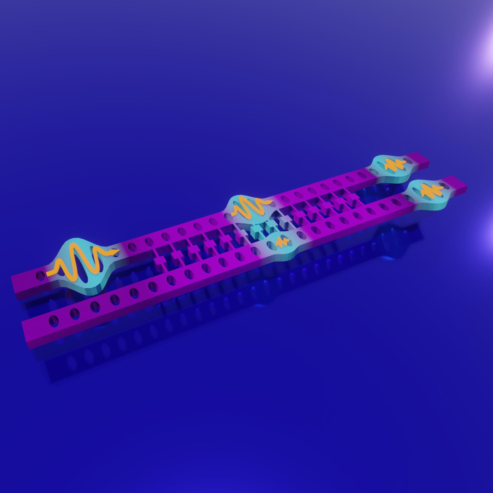
Ultrathin structures that can bend, focus, or filter light, metasurfaces are reshaping how scientists think about optics. These engineered materials offer precise control over lights behavior, but many conventional designs are held back by inefficiencies. Typically, they rely on local resonances within individual nanostructures, which often leak energy or perform poorly at wide angles. These shortcomings limit their usefulness in areas like sensing, nonlinear optics, and quantum technologies.

A growing area of research looks instead to nonlocal metasurfaces, where interactions between many elements create collective optical effects. These collective behaviors can trap light more efficiently, producing sharper resonances and stronger interactions with matter. One of the most promising possibilities in this field is the development of photonic flatbands, where resonant behavior stays uniform across a wide range of viewing angles.

Another is creating chiral responses, which allow devices to distinguish between left-and right-handed circularly polarized light. Until now, however, achieving both flatband and chiral behavior with high efficiency on a single platform has remained a major challenge.

Quantum uncertainty captured in real time using femtosecond light pulses

Researchers from the University of Arizona, working with an international team, have captured and controlled quantum uncertainty in real time using ultrafast pulses of light. Their discovery, published in the journal Light: Science & Applications, could lead to more secure communication and the development of ultrafast quantum optics.

At the heart of the breakthrough is “squeezed light,” said Mohammed Hassan, the paper’s corresponding author and associate professor of physics and optical sciences.

In , light is identified by two linked properties that roughly correspond to a particle’s position and intensity—but can never be known with perfect precision, a concept known as uncertainty. The product of these two measurements cannot fall below a certain threshold, much like the fixed amount of air in a balloon, with each measurement representing one side of the balloon.

Researchers develop the first miniaturized ultraviolet spectrometer chip

Recently, the iGaN Laboratory led by Professor Haiding Sun at the School of Microelectronics, University of Science and Technology of China (USTC), together with the team of academician Sheng Liu from Wuhan University, has successfully developed the world’s first miniaturized ultraviolet (UV) spectrometer chip and realized on-chip spectral imaging.

Based on a novel gallium nitride (GaN) cascaded photodiode architecture and integrated with (DNN) algorithms, the device achieves high-precision spectral detection and high-resolution multispectral imaging.

With a response speed on the nanosecond scale, it sets a new world record for the fastest reported miniaturized spectrometer. The work, titled “A miniaturized cascaded-diode-array spectral imager,” was published online in Nature Photonics on September 26, 2025.

Stretchable waveguides maintain stable transmission even when bent or twisted

Researchers have designed and demonstrated stretchable waveguides that maintain efficient, stable signal transmission of surface plasmon polaritons even when bent, twisted or stretched. These plasmonic waveguides could make it possible to seamlessly embed advanced sensing, communication and health monitoring functions into everyday wearable materials.

Plasmonic waveguides are tiny structures that guide light by coupling it with electrons on a . The new flexible waveguides transmit what are known as spoof surface plasmon polaritons, which are formed with in this case—rather than the conventional infrared or .

“Although our work is still at the research stage, it highlights the exciting possibility of merging advanced electromagnetic technologies with soft, stretchable materials,” said research team leader Zuojia Wang from Zhejiang University. “This brings us closer to a future where advanced health care and connectivity are integrated into what we wear.”

Cryo-imaging gives deeper view of thick biological materials

Electron microscopy is an exceptional tool for peering deep into the structure of isolated molecules. But when it comes to imaging thicker biological samples to understand how those molecules function in their cellular environments, the technology gets a little murky.

Cornell researchers devised a new method, called tilt-corrected bright-field scanning transmission electron microscopy (tcBF-STEM), to image thick samples with higher contrast and a fivefold increase in efficiency.

The Sept. 23 publication of the findings, in Nature Methods, arrives two years after the death of co-author Lena Kourkoutis, M.S. ‘06, Ph.D. ‘09, associate professor in applied and in Cornell Engineering, whose work in cryo-electron microscopy drove much of the nearly 10-year effort.

Map of bacterial gene interactions uncovers targets for future antibiotics

Despite rapid advances in reading the genetic code of living organisms, scientists still face a major challenge today—knowing a gene’s sequence does not automatically reveal what it does. Even in simple, well-studied bacteria like Escherichia coli (better known as E. coli), about one-quarter of the genes have no known function. Traditional approaches—turning off one gene at a time and studying the effects—are slow, laborious, and sometimes inconclusive due to gene redundancy.

Researchers from the Yong Loo Lin School of Medicine, National University of Singapore (NUS Medicine) and collaborators from the University of California, Berkeley (UC Berkeley) have developed a new technique called Dual transposon sequencing (Dual Tn-seq), which allows for rapid identification of genetic interactions. It maps how bacterial genes work together, revealing vulnerabilities that could be targeted by future antibiotics.

“This is like mapping the social network for ,” said Assistant Professor Chris Sham Lok To from the Infectious Diseases Translational Research Program and the Department of Microbiology and Immunology, NUS Medicine, who led the study. “We can now see which genes depend on each other, and which pairs of genes bacteria can’t live without. That’s exactly the insight we need for next-generation antibiotics.”

From engines to nanochips: Physicists redefine how heat really moves

Heat has always been something we thought we understood. From baking bread to running engines, the idea seemed simple: heat spreads out smoothly, like water soaking through a sponge. That simple picture, written down by Joseph Fourier 200 years ago, became the foundation of modern science and engineering.

But zoom into the nanoscale—inside the chips that power your smartphone, AI hardware, or next-generation solar panels—and the story changes. Here, heat doesn’t just “diffuse.” It can ripple like , remember its past, or flow in elegant streams like a fluid in a pipe. For decades, scientists had pieces of this puzzle but no unifying explanation.

Now, researchers at Auburn University and the U.S. Department of Energy’s National Renewable Energy Laboratory have delivered what they call a “unified statistical theory of heat conduction.”

Third dimension of data storage: Physicists demonstrate first hybrid skyrmion tubes for higher-density quantum computing

Typically, the charge of electrons is used to store and process information in electronics-based devices. In spintronics, the focus is instead on the magnetic moment or on magnetic vortices, so-called skyrmions—the goal is smaller, faster, and more sustainable computers. To further increase storage density, skyrmions will not only be two-dimensional in the future, but will also conquer the third dimension.

Researchers from the Institute of Physics at Johannes Gutenberg University Mainz (JGU) have now succeeded in creating three-dimensional skyrmions, so-called hybrid skyrmion tubes, in synthetic antiferromagnets and have demonstrated for the first time that these skyrmion tubes move differently than two-dimensional skyrmions.

“Three-dimensional skyrmions are of interest for and brain-inspired computing, among other things—here the higher resulting from the third dimension is essential,” says Mona Bhukta from Professor Mathias Kläui’s research group. The results were published on September 26 in Nature Communications.

Harnessing GeSn semiconductors for tomorrow’s quantum world

An international team of researchers from Forschungszentrum Jülich (Germany), Tohoku University (Japan), and École Polytechnique de Montréal (Canada) has made a significant discovery in semiconductor science by revealing the remarkable spin-related material properties of Germanium-Tin (GeSn) semiconductors.

Semiconductors control the flow of electricity that power everyday technology all around us (such as cars and computers). However, technology is progressing at such a breakneck speed that it is straining current technologies.

“Semiconductors are approaching their physical and energy-efficiency limits in terms of speed, performance, and ,” says Makoto Kohda from Tohoku University. “This is a huge issue because we need semiconductors that can keep up as we shift to more demanding needs such as 5G/6G networks and the increased use of artificial intelligence.”

Chip-based phonon splitter brings hybrid quantum networks closer to reality

Researchers have created a chip-based device that can split phonons—tiny packets of mechanical vibration that can carry information in quantum systems. By filling a key gap, this device could help connect various quantum devices via phonons, paving the way for advanced computing and secure quantum communication.

“Phonons can serve as on-chip quantum messages that connect very different quantum systems, enabling hybrid networks and new ways to process in a compact, scalable format,” said research team leader Simon Gröblacher from Delft University of Technology in the Netherlands.

“To build practical phononic circuits requires a full set of chip-based components that can generate, guide, split and detect individual quanta of vibrations. While sources and waveguides already exist, a compact splitter was still missing.”

/* */