We may be on the cusp of an era of astonishing innovation — the limits of which aren’t even clear yet.


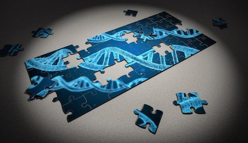
MIT and Dana-Farber Cancer Institute have teamed up to create an AI model that CRACKS the code of mysterious cancer origins! No more guesswork-this model predicts where tumors come from with up to 95% accuracy. For more insight, visit https://www.channelchek.com #Cancer #CancerBreakthrough #AIinMedicine #MedicalScience #BioTech #FutureOfHealthcare #FightCancer #HealthTech #CancerResearch #PrecisionMedicine
Try free for 7 days, and get a 60% discount if you join the Speakly annual subscription: https://speakly.app.link/sciencephile…
Sciencephile Merch: https://crowdmade.com/collections/sci…
Support me at Patreon: / sciencephiletheai.
Facebook: / sciencephile.
Twitter: / sciencephile_
Reddit: / sciencephiletheai.
Researchers at CHU Sainte-Justine and Université de Montréal have discovered a new mechanism involved in the expression of Down syndrome, one of the main causes of intellectual disability and congenital heart defects in children. The study’s findings were published today in Current Biology.
Down syndrome (SD), also called trisomy 21 syndrome, is a genetic condition that affects approximately one in every 800 children born in Canada. In these individuals, many genes are expressed abnormally at the same time, making it difficult to determine which genes contribute to which differences.
Professor Jannic Boehm’s research team focused on RCAN1, a gene that is overexpressed in the brains of fetuses with Down syndrome. The team’s work provides insights into how the gene influences the way the condition manifests itself.
AI systems, such as GPT-4, can now learn and use human language, but they learn from astronomical amounts of language input—much more than children receive when learning how to understand and speak a language. The best AI systems train on text with a word count in the trillions, whereas children receive just millions per year.
Due to this enormous data gap, researchers have been skeptical that recent AI advances can tell us much about human learning and development. An ideal test for demonstrating a connection would involve training an AI model, not on massive data from the web, but on only the input that a single child receives. What would the model be able to learn then?
A team of New York University researchers ran this exact experiment. They trained a multimodal AI system through the eyes and ears of a single child, using headcam video recordings from when the child was 6 months and through their second birthday. They examined if the AI model could learn words and concepts present in a child’s everyday experience.
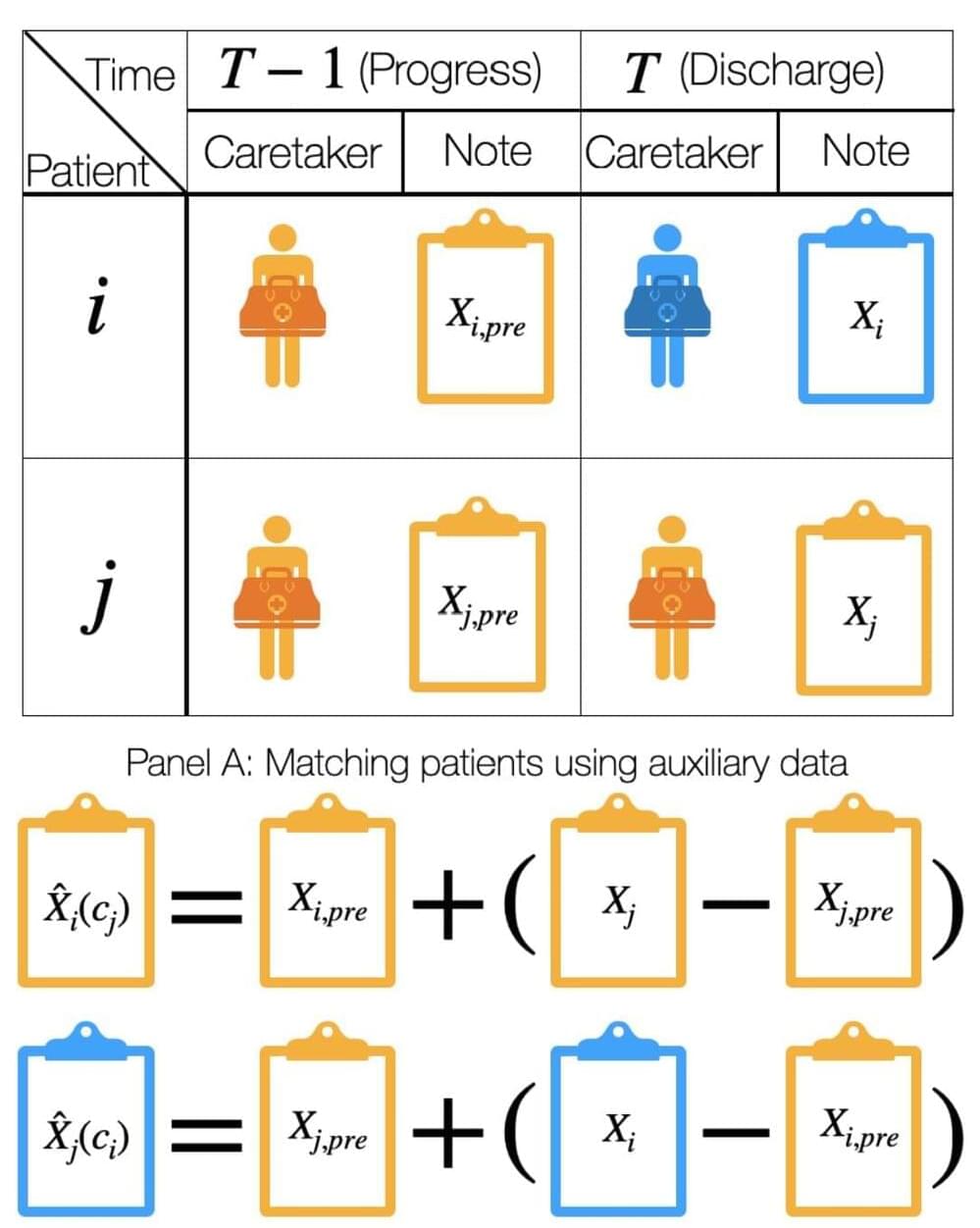
The amount of digital data available is greater than ever before, including in health care, where doctors’ notes are routinely entered into electronic health record systems. Manually reviewing, analyzing, and sorting all these notes requires a vast amount of time and effort, which is exactly why computer scientists have developed artificial intelligence and machine learning techniques to infer medical conditions, demographic traits, and other key information from this written text.
However, safety concerns limit the deployment of such models in practice. One key challenge is that the medical notes used to train and validate these models may differ greatly across hospitals, providers, and time. As a result, models trained at one hospital may not perform reliably when they’re deployed elsewhere.
Previous seminal works by Johns Hopkins University’s Suchi Saria—an associate professor of computer science at the Whiting School of Engineering—and researchers from other top institutions recognize these “dataset shifts” as a major concern in the safety of AI deployment.
Saint Louis University associate professor of health management and policy in the College for Public Health and Social Justice, SangNam Ahn, Ph.D., recently published a paper in Journal of Clinical Psychology that examines the relationship between childhood adversity, and psychiatric decline as well as adult adversity and psychiatric and cognitive decline.
His team discovered that just one instance of adversity in childhood can increase cases of mental illness later in life, and adverse events in adults can lead to a greater chance of both mental illness and cognitive decline later in life.
“Life is very complicated, very dynamic,” Ahn said. “I really wanted to highlight the importance of looking into the lasting health effect of adversity, not only childhood but also adulthood adversity on health outcomes, especially physical health and psychiatric and cognitive health. There have been other studies before, but this is one of the first that looks into these issues comprehensively.”
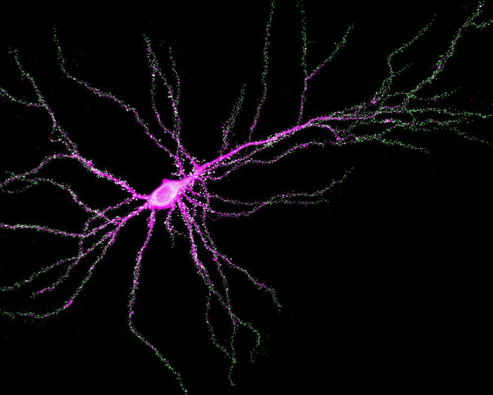
Johns Hopkins Medicine neuroscientists say they have found a new function for the SYNGAP1 gene, a DNA sequence that controls memory and learning in mammals, including mice and humans.
The finding, published in Science, may affect the development of therapies designed for children with SYNGAP1 mutations, who have a range of neurodevelopmental disorders marked by intellectual disability, autistic-like behaviors, and epilepsy.
In general, SYNGAP1, as well as other genes, control learning and memory by making proteins that regulate the strength of synapses—the connections between brain cells.