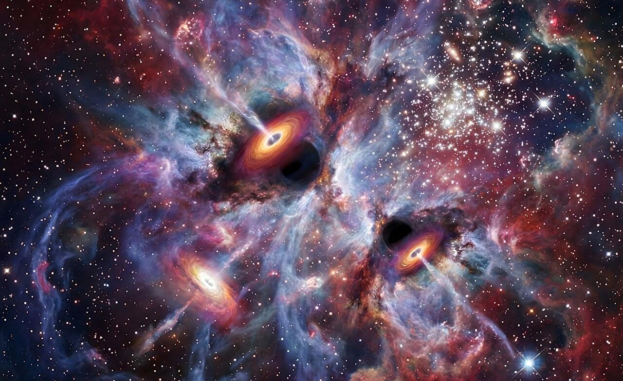
Toggle light / dark theme

Get the latest international news and world events from around the world.

Log in for authorized contributors

Dr. Norman Putzki, MD — Novartis — Gene Therapy And A New Era Of Neuroscience

Gene Therapy And A New Era Of Neuroscience — Dr. Norman Putzki, MD — SVP, Global Clinical Development Head, and U.S. Development Site Head, Novartis.


Dr. Norman Putzki, MD is Senior Vice President, Global Clinical Development Head, and U.S. Development Site Head at Novartis (https://www.novartis.com/) where he oversees global teams working on next-generation gene therapies, RNA-based medicines, targeted biologics, and innovative small molecules.

Dr. Putzki most recently served as Global Head of Development for Neuroscience and Gene Therapy at Novartis, where he oversaw one of the world’s most ambitious pipelines aimed at transforming the lives of patients with neurological, neuromuscular, and rare genetic diseases.

A physician–scientist by training, with an MD from University of Duisburg Essen, Dr. Putzki has built a career at the intersection of clinical medicine, translational research, and large-scale drug development.

Before joining Novartis, Dr. Putzki led programs across multiple therapeutic areas at Biogen Idec and has played key roles in advancing clinical treatments for conditions long considered intractable including MS and Parkison’s disease.

How to build a genome: Scientists release troubleshooting manual for synthetic life

Leading synthetic biologists have shared hard-won lessons from their decade-long quest to build the world’s first synthetic eukaryotic genome in a Nature Biotechnology paper. Their insights could accelerate development of the next generation of engineered organisms, from climate-resilient crops to custom-built cell factories.

“We’ve assembled a comprehensive overview of the literature on how to build a lifeform where we review what went right—but also what went wrong,” says Dr. Paige Erpf, lead author of the paper and postdoctoral researcher at Macquarie University’s School of Natural Sciences and the Australian Research Council (ARC) Center of Excellence in Synthetic Biology.

The Synthetic Yeast Genome Project (Sc2.0) involved a large, evolving global consortium of 200-plus researchers from more than ten institutions, who jointly set out to redesign and chemically synthesize all 16 chromosomes of baker’s yeast from scratch. Macquarie University contributed to the synthesis of two of these chromosomes, comprising around 12% of the project overall.

Growth strategy enables coherent quantum transport in single-layer MoS₂ semiconductors

Two-dimensional (2D) semiconductors are thin materials (i.e., one-atom thick) with advantageous electronic properties. These materials have proved to be promising for the development of thinner, highly performing electronics, such as fitness trackers and portable devices.

A 2D semiconductor that has attracted particular interest within the electronics community is molybdenum disulfide (MoS₂), a transition-metal dichalcogenide made up of one metal atom and two chalcogen atoms. To build reliable large-area electronics based on MoS₂ layers, engineers need to uniformly grow this material over wafer-scale surfaces, minimizing defects that hinder the performance of devices.

Researchers at the Institute for Basic Science (IBS), Pohang University of Science and Technology (POSTECH) and other institutes recently introduced a new approach to grow single-layer MoS₂ on substrates while maintaining a uniform atomic arrangement. Their approach, outlined in a paper in Nature Electronics, entails a greater control of the process by which small crystal regions merge on a substrate, also known as coalescence.

Two-step method enables controllable WS₂ epitaxy growth

In a study published in Journal of the American Chemical Society, a team led by Prof. Song Li from the University of Science and Technology of China (USTC) of the Chinese Academy of Sciences synthesized monolayer WS2 lateral homojunctions via in situ domain engineering, and enabled controllable direct chemical vapor deposition (CVD) growth of these structures.

Two-dimensional (2D) are ideal candidates to replace silicon-based semiconductors due to their exceptional electrical properties at atomic scales. However, device applications require heterogeneous field-effect modulation behaviors across low-dimensional units. Van der Waals interactions or lateral atomic bonding allow damage-free integration into homojunctions/heterojunctions, but direct epitaxy growth remains challenging due to strict atomic species constraints.

In this study, researchers first determined optimal intrinsic defect configurations through theoretical simulations. Then they employed a two-step CVD method to achieve the in situ modulation of defect structures at the domain level, yielding homojunctions with tailored defect architectures.

Epitaxial multilayer MoS2 wafers promise high-performance transistors

Two-dimensional (2D) semiconductors, such as molybdenum disulfide (MoS2), enable unprecedented opportunities to solve the bottleneck of transistor scaling and to build novel logic circuits with faster speeds, lower power consumption, flexibility and transparency, benefiting from their ultra-thin thickness, dangling-bond-free flat surface and excellent gate controllability.

Tremendous efforts have been devoted to exploring the scaled-up potentials of MoS2, including both wafer-scale synthesis of high-quality materials and large-area devices. For instance, four-inch wafer-scale monolayer MoS2 with large domain sizes (up to ~300 μm) and record-high electronic quality (average field-effect mobility of ~80 cm2·V-1 ·s-1) has already been demonstrated via van der Waals epitaxial growth.

In terms of a further improvement of the electronic quality of the large-scale monolayer MoS2, structural imperfections should be eliminated as much as possible; however, there is not much space left for monolayer MoS2 after ten years of synthesis optimizations in this field. Another key direction is to switch to multilayer MoS2, e.g., bilayers and trilayers, since they have intrinsically higher electronic quality than monolayers and thus are conducive to higher-performance devices and logic circuits. However, due to the fundamental limitation of thermodynamics, it is still a great challenge to realize wafer-scale multilayer MoS2 with high-quality and large-scale uniformity.

Real-life ‘quantum molycircuits’ using exotic nanotubes

Molybdenum disulfide MoS2 is a groundbreaking material for electronics applications. As a two-dimensional layer similar to graphene, it is an excellent semiconductor, and can even become intrinsically superconducting under the right conditions. It’s not particularly surprising that science fiction authors have already been speculating about molycircs, fictional computer circuits built from MoS2, for years—and that physicists and engineers are directing huge research efforts at this material.

Researchers at the University of Regensburg, have many years of expertise with diverse quantum materials—in particular also with carbon nanotubes, tube-like macromolecules made from carbon atoms alone.

“It was an obvious next step to now focus on MoS2 and its fascinating properties,” said Dr. Andreas K. Hüttel, head of the research group Nanotube Electronics and Nanomechanics in Regensburg. In cooperation with Prof. Dr. Maja Remškar, Jožef Stefan Institut Ljubljana, a specialist in the crystalline growth of nanomaterials, his research group started working on based on MoS2 nanotubes.

New method realize ohmic contacts in n-type MoS₂ transistors at cryogenic temperatures

Semiconducting transition metal dichalcogenides (TMDs) are a class of layered materials exhibiting unique optoelectronic properties that could be leveraged to develop transistors, sensors and other nanoelectronics. Despite their advantages, creating robust ohmic contacts that connect a metal electrode in transistors to semiconducting TMDs at cryogenic temperatures has proved challenging.

This has so far limited the use of these materials for either studying or developing nanoelectronics that operate at low temperatures.

In a paper in Nature Electronics, researchers at the Liaoning Academy of Materials, Shanxi University and other institutes introduced a new technique for realizing ohmic contacts to the TMD molybdenum disulfide (MoS2) at , and found that in those transistors can be surprisingly high.

Graphene membranes offer efficient, low-cost option for industrial CO₂ capture

Carbon capture is becoming essential for industries that still depend on fossil fuels, including the cement and steel industries. Natural-gas power plants, coal plants, and cement factories all release large amounts of CO₂, and reducing those emissions is difficult without dedicated capture systems. Today, most plants rely on solvent-based systems that absorb CO₂, but these setups use a lot of heat, require major infrastructure, and can be costly to run.

A smaller, electricity-driven alternative is what the field calls a “membrane” system. A membrane works like an ultra-fine filter that lets certain gases slip through more easily than others, separating CO₂ from the rest of the flue gas. The problem is that many membranes lose efficiency when CO₂ levels are low, which is common in natural-gas plants, and this limits where they can be used.

A new study at EPFL has now analyzed how a new membrane material, pyridinic-graphene, could work at scale. This is a single-layer graphene sheet with tiny pores that favor CO₂ over other gases. The researchers combined experimental performance data with modeling tools that simulate real operating conditions, such as energy use and gas flow. They also explored a wide range of cost scenarios to see how the material might behave once deployed in commercial plants.

/* */