Fabricating some structures using niobium instead of aluminum could lead to more resilient superconducting quantum computers.

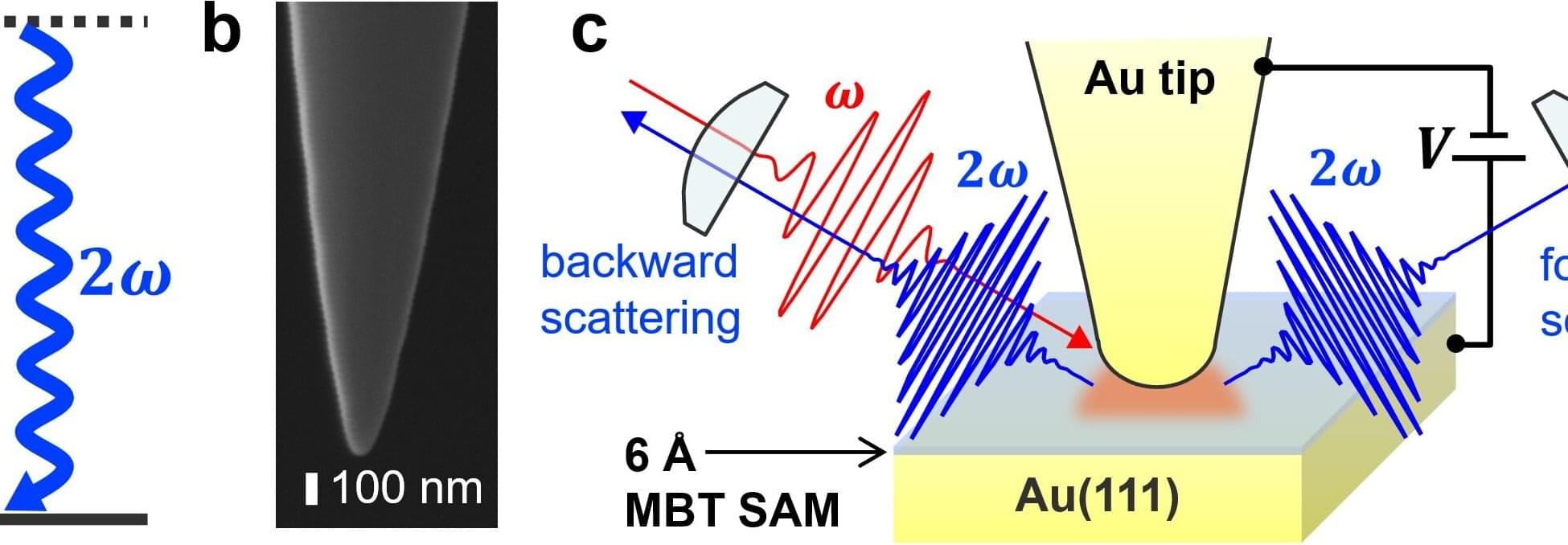
Researchers at the Institute for Molecular Science (NINS, Japan) and SOKENDAI have demonstrated a more than 2000% voltage-induced enhancement of near-field nonlinear optical responses. To achieve this giant modulation, they focused on an angstrom-scale gap formed between a metallic tip and substrate in a scanning tunneling microscope (STM), which can strongly confine and enhance light intensity through plasmon excitation. The paper is published in the journal Nature Communications.
The researchers discovered that when the voltage across the junction was varied within ±1 V, the intensity of second-harmonic generation (SHG) changed quadratically with voltage and exhibited giant modulation with a depth of ~2000%/V. This represents a more than two-orders-of-magnitude improvement over previous electroplasmonic systems.
Moreover, similar giant electrical modulation was also observed for sum-frequency generation, a nonlinear optical process that upconverts mid-infrared light into visible or near-infrared light. This demonstrates that the newly discovered electrical modulation mechanism is applicable to the broad spectral range, not limited to a specific optical wavelength or nonlinear optical process.
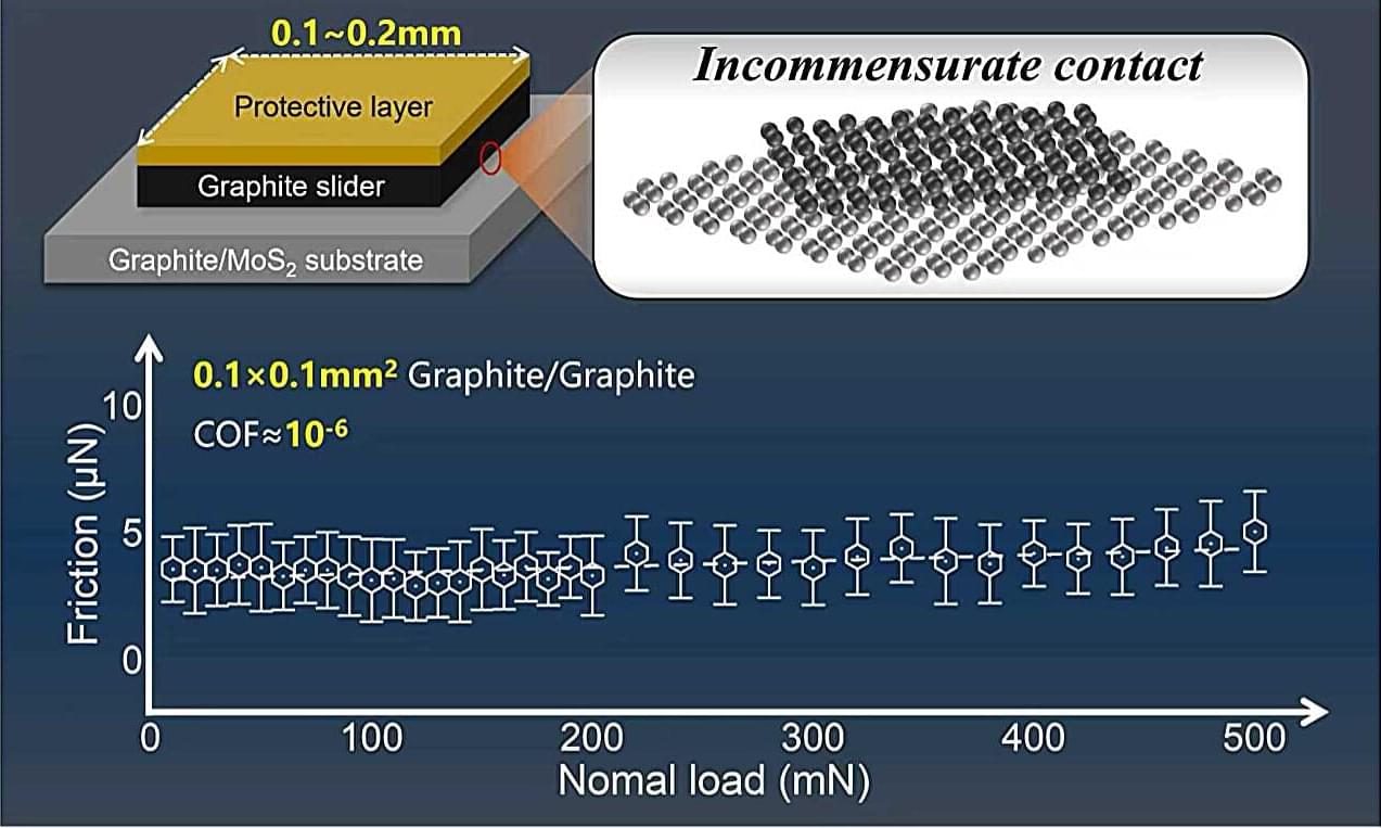
For the first time, physicists in China have virtually eliminated the friction felt between two surfaces at scales visible to the naked eye. In demonstrating “structural superlubricity,” the team, led by Quanshui Zheng at Tsinghua University, have resolved a long-standing debate surrounding the possibility of the effect. Published in Physical Review Letters, the result could potentially lead to promising new advances in engineering.
When two objects slide over each other, any roughness on their surfaces will almost inevitably resist the motion, creating the force of friction. Yet in 2004, physicists showed that friction can be virtually eliminated between two graphite surfaces, simply by rotating their respective molecular structures.
Named structural superlubricity (SSL), the effect is highly desired by engineers; in principle, allowing them to eliminate wear on both surfaces and minimize energy lost as waste heat.
In 2023, a subatomic particle called a neutrino crashed into Earth with such a high amount of energy that it should have been impossible. In fact, there are no known sources anywhere in the universe capable of producing such energy—100,000 times more than the highest-energy particle ever produced by the Large Hadron Collider, the world’s most powerful particle accelerator. However, a team of physicists at the University of Massachusetts Amherst recently hypothesized that something like this could happen when a special kind of black hole, called a “quasi-extremal primordial black hole,” explodes.
In new research published in Physical Review Letters, the team not only accounts for the otherwise impossible neutrino but shows that the elementary particle could reveal the fundamental nature of the universe.

As commercial spaceflight draws ever closer and time spent in space continues to extend, the question of reproductive health beyond the bounds of planet Earth is no longer theoretical but now “urgently practical,” according to a new study published in the journal Reproductive Biomedicine Online.
“More than 50 years ago,” explains clinical embryologist Giles Palmer from the International IVF Initiative Inc, “two scientific breakthroughs reshaped what was thought biologically and physically possible—the first moon landing and the first proof of human fertilization in vitro.
Now, more than half a century later, we argue in this report that these once-separate revolutions are colliding in a practical and underexplored reality: space is becoming a workplace and a destination, while assisted reproductive technologies have become highly advanced, increasingly automated and widely accessible.
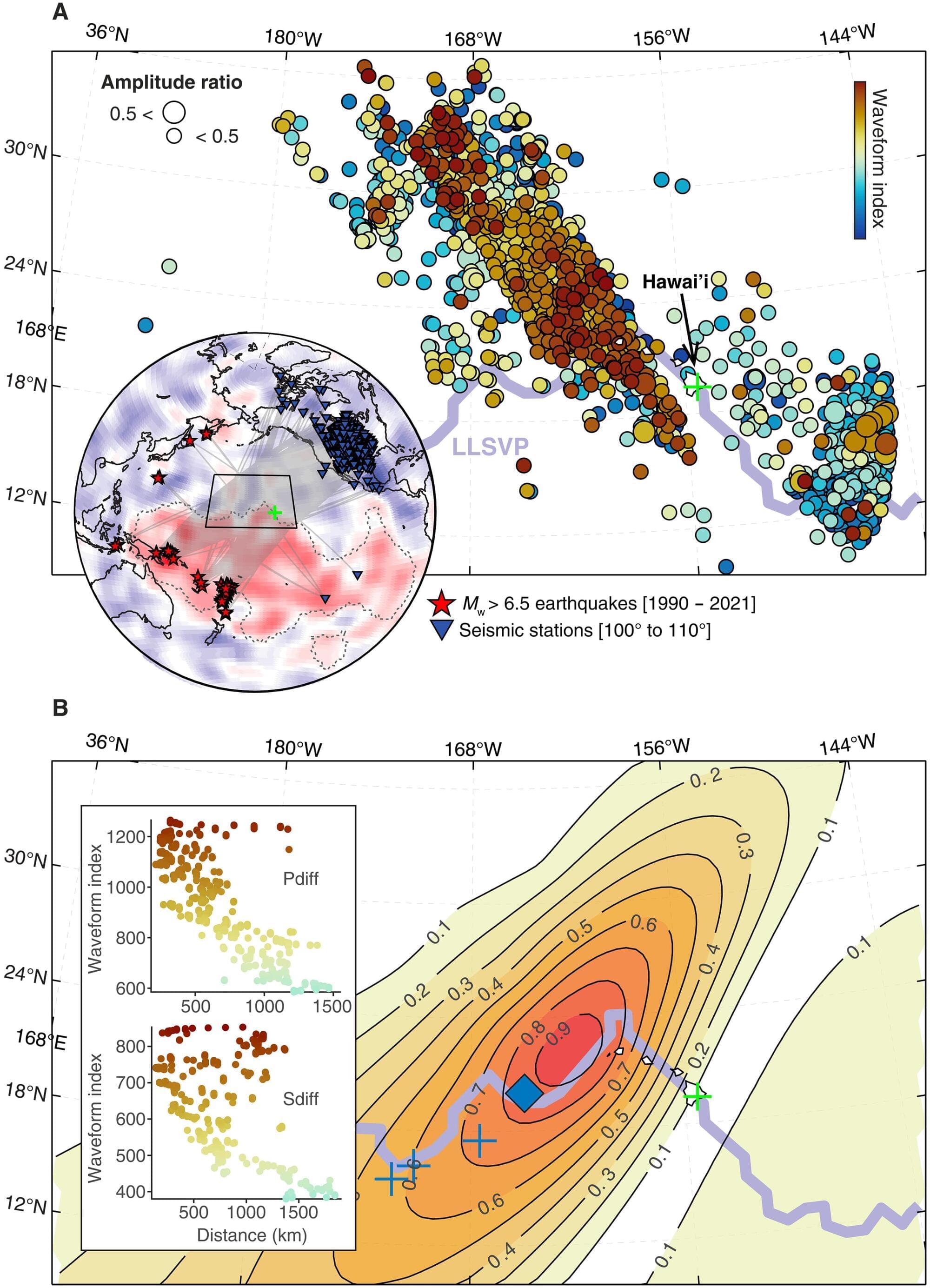
Mantle plumes beneath volcanic hotspots, like Hawaii, Iceland, and the Galapagos, seem to be anchored into a large structure within the core-mantle boundary (CMB). A new study, published in Science Advances, takes a deeper dive into the structure under Hawaii using P-and S-wave analysis and mineralogical modeling, revealing its composition and properties.
It is known that anomalous structures exist within Earth’s lower mantle, including large low-velocity provinces (LLVPs) and ultra low-velocity zones (ULVZs), which cause seismic waves to slow down dramatically. Larger ULVZs, typically referred to as mega-ultra low velocity zones, are found near the CMB and often beneath oceanic hotspots like Hawaii. Mega-ULVZs can be over several hundred kilometers in length. Previous studies have linked these megastructures to mantle plumes and some say they may preserve primordial geochemical signatures.
However, current tomographic methods have been unable to fully analyze mega-ULVZs, and their composition and origin remain unclear. Seismic waves, on the other hand, present a way to investigate ULVZs, largely due to the effect ULVZs have on wave velocity.
Quantum technologies, devices and systems that process, store, detect, or transfer information leveraging quantum mechanical effects, have the potential to outperform classical technologies in a variety of tasks. An ongoing quest within quantum engineering is the realization of a so-called quantum internet: a network conceptually analogous to today’s internet, in which distant nodes are linked through shared quantum resources, most notably quantum entanglement.
Researchers at Nanjing University and University of Science and Technology of China have developed a new ultra-thin metasurface that could contribute to this goal, as it can control the behavior of light, while also generating and directing entanglement across many channels.
This metasurface, presented in a paper published in Physical Review Letters, has so far proved to be promising for the development of scalable and integrated quantum technologies.

Researchers at the Department of Energy’s Oak Ridge National Laboratory are breathing new life into the scientific understanding of neptunium, a unique, radioactive, metallic element—and a key precursor for production of the plutonium-238, or Pu-238, that fuels exploratory spacecraft.
The ORNL team’s research arrives during a period of increased national interest in the use of Pu-238 in radioisotope thermoelectric generators, or RTGs. Often used in space missions such as NASA’s Perseverance Rover for long-term power, RTGs convert heat from radioactive decay into electricity. Advancing RTG knowledge and application possibilities also requires the same high-level evaluation of both chemical reactions and structural characterization, two key aspects of the materials science for which ORNL is known.
“When people want to do scientific experiments in space, they need something to power their instruments, and plutonium is typically the power source because things like solar and lithium ion batteries don’t withstand deep space,” said Kathryn Lawson, radiochemist in ORNL’s Fuel Cycle Chemical Technology Group and lead author of the new study.
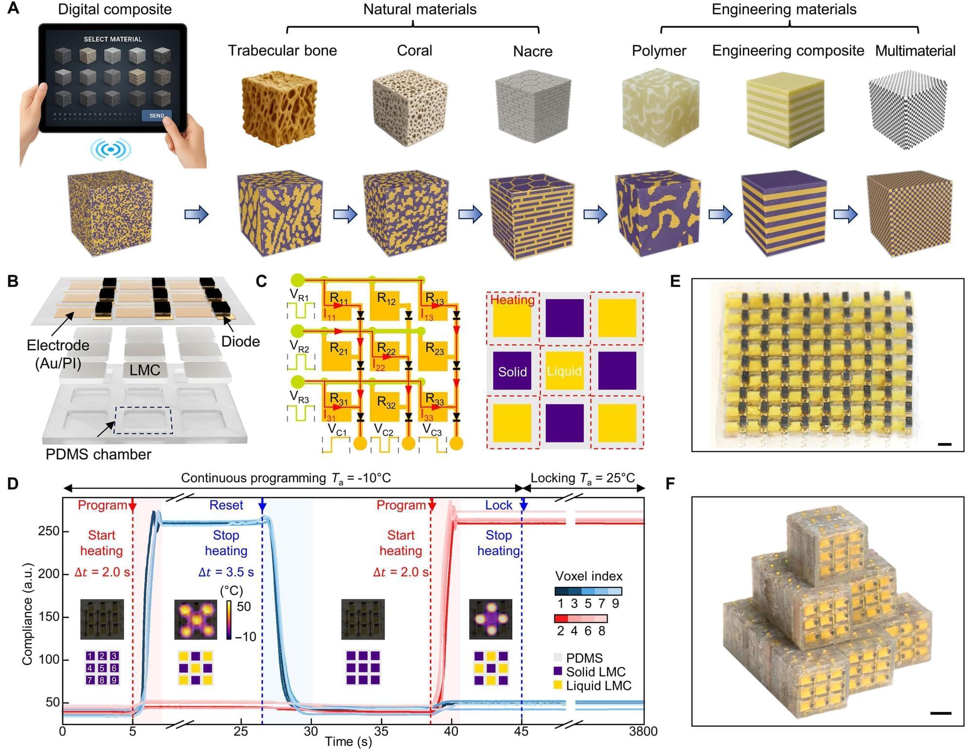
Mechanical engineers at Duke University have demonstrated a proof-of-concept method for programming mechanical properties into solid Lego-like building blocks. By controlling the solidity of hundreds of individual cells in specific patterns, the approach could allow futuristic robotics to alter their mechanical properties and functionalities on the fly.
In their initial tests, the researchers showed how a tail-like 3D beam with various configurations can move a robotic fish through water along different paths with the same motor activity. The team envisions miniaturized versions of the technology that could, for example, maneuver through blood vessels to survey their health or even reconfigure to form an adaptive stent.
The research appears in the journal Science Advances.
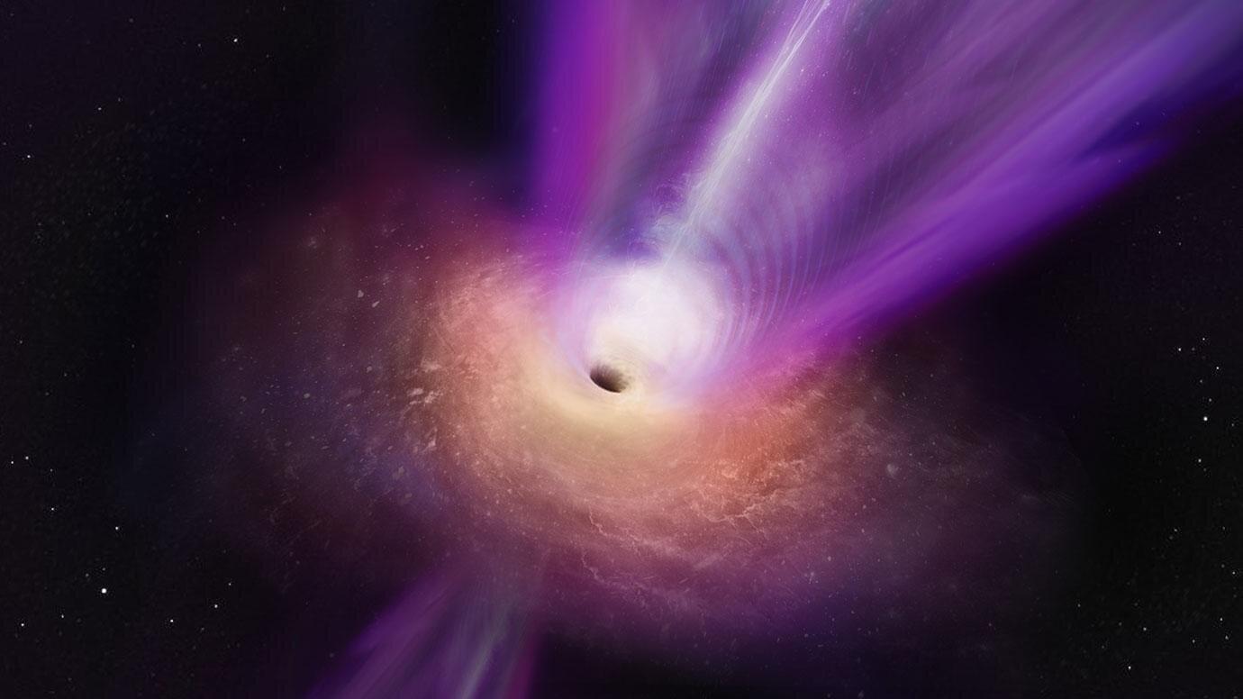
Gigantic black holes lurk at the center of virtually every galaxy, including ours, but we’ve lacked a precise picture of what impact they have on their surroundings. However, a University of Chicago-led group of scientists has used data from a recently launched satellite to reveal our clearest look yet into the boiling, seething gas surrounding two supermassive black holes, each located in the center of massive galaxy clusters.
“For the first time, we can directly measure the kinetic energy of the gas stirred by the black hole,” said Annie Heinrich, UChicago graduate student and among the lead authors on one of two papers on the findings, released in Nature. “It’s as though each supermassive black hole sits in the ‘eye of its own storm.’”
The readings came from the satellite XRISM, which was launched in 2023 by the Japanese Aerospace Exploration Agency in partnership with NASA and the European Space Agency. It has a unique ability to track the motions and read the chemical makeup of extremely hot, X-ray emitting gas in galaxy clusters.