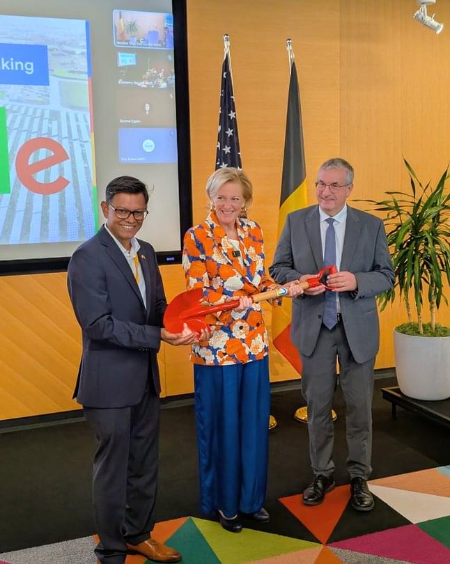
Google is investing an additional €5 billion in Belgium over the next two years to expand its cloud and AI infrastructure. This includes expansions of our data center campuses in Saint-Ghislain and will add another 300 full time jobs. We’ve also announced new agreements with Eneco, Luminus and Renner which will support the development of new onshore wind farms and support the grid with clean energy.
Our commitment goes beyond infrastructure. We’re also equipping Belgians with the skills needed to thrive in an AI-driven economy, at no cost and will fund non-profits to provide free, practical AI training for low-skilled workers.
This is an extraordinary time for European innovation and its digital and economic future. Google is deepening its roots in Belgium and investing in its residents to unlock significant economic opportunities for the country, helping to ensure it remains a leader in technology and AI.
Orbiting between Mars and Jupiter lies the asteroid belt, a vast region of space populated by approximately 1.9 million asteroids, each over one kilometer in
What a difference a year makes! Today Hera’s asteroid mission for planetary defence is cruising through deep space on the far side of the Sun, headed to its final destination: the Didymos binary asteroid system. But a year ago, on 7 October 2024, it was unsure if the mission was ever going to take off at all.
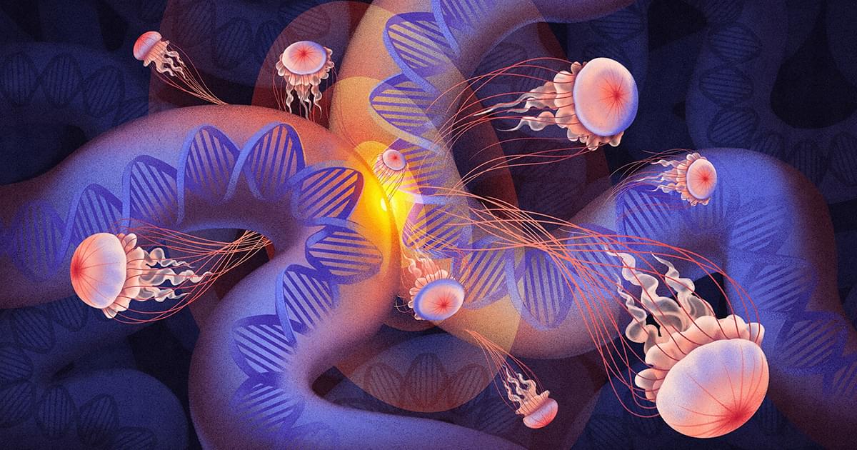
Since Madeline Lancaster first created brain organoids back in 2013, they have become widely used for brain research around the world. But what exactly are they? Are they effectively miniature brains in dishes? Could implanting them in animals create super-smart mice? How close are we to crossing ethical lines? Michael Le Page visited Lancaster at her lab at the MRC Laboratory of Molecular Biology in Cambridge, UK, to find out.
Learn more ➤ https://www.newscientist.com/article/.… ➤ https://bit.ly/NSYTSUBS Get more from New Scientist: Official website: https://bit.ly/NSYTHP Facebook: https://bit.ly/NSYTFB Twitter: https://bit.ly/NSYTTW Instagram: https://bit.ly/NSYTINSTA LinkedIn: https://bit.ly/NSYTLIN About New Scientist: New Scientist was founded in 1956 for “all those interested in scientific discovery and its social consequences”. Today our website, videos, newsletters, app, podcast and print magazine cover the world’s most important, exciting and entertaining science news as well as asking the big-picture questions about life, the universe, and what it means to be human. New Scientist https://www.newscientist.com/ 00:00 Introduction 00:54 Making the first brain organoid 01:52 What are brain organoids? 03:12 What makes our brains unique? 04:08 Modelling disease 07:01 Transplanting organoids into animals 10:41 Could we make full-sized brains? 13:19 Are brain organoids conscious? 15:21 Ethical guidelines.
About New Scientist: New Scientist was founded in 1956 for “all those interested in scientific discovery and its social consequences”. Today our website, videos, newsletters, app, podcast and print magazine cover the world’s most important, exciting and entertaining science news as well as asking the big-picture questions about life, the universe, and what it means to be human.
Painting walls in light colors, insulating roofs, choosing medium-sized windows, and aligning buildings to the sun’s path may seem like simple choices. But they could provide powerful defenses against climate change for millions of people in the world’s most vulnerable regions.
That’s the message of a study, appearing in the journal Energy and Buildings, which identifies low-cost, climate-smart design strategies as crucial for future housing in Latin America’s rapidly warming cities.
Researchers used computer simulations to test how various climate-resilient building projects would perform under current and projected climate conditions in five major cities—Rio de Janeiro and São Paulo, in Brazil, Santiago (Chile), Bogotá (Colombia), and Lima (Peru).
🤖 How far can AI go? Jeff Crume examines generative AI, NLP, and AGI, unpacking solved milestones like reasoning and creativity while tackling ongoing challenges like hallucinations and sustainability. Learn about the limits of AI and its role alongside humans in shaping the future.
AI news moves fast. Sign up for a monthly newsletter for AI updates from IBM → https://ibm.biz/Bde7Sz.
Researchers from NC State University have identified the first hardware vulnerability that allows attackers to compromise the data privacy of artificial intelligence (AI) users by exploiting the physical hardware on which AI is run.
The paper, “GATEBLEED: A Timing-Only Membership Inference Attack, MoE-Routing Inference, and a Stealthy, Generic Magnifier Via Hardware Power Gating in AI Accelerators,” will be presented at the IEEE/ACM International Symposium on Microarchitecture (MICRO 2025), being held Oct. 18–22 in Seoul, South Korea. The paper is currently available on the arXiv preprint server.
“What we’ve discovered is an AI privacy attack,” says Joshua Kalyanapu, first author of a paper on the work and a Ph.D. student at North Carolina State University. “Security attacks refer to stealing things actually stored somewhere in a system’s memory—such as stealing an AI model itself or stealing the hyperparameters of the model. That’s not what we found. Privacy attacks steal stuff not actually stored on the system, such as the data used to train the model and attributes of the data input to the model. These facts are leaked through the behavior of the AI model. What we found is the first vulnerability that allows successfully attacking AI privacy via hardware.”