The world’s most famous genetic tool has a major diversity problem.


It appears that researchers in China have facilitated the birth of the first “designer baby” – actually babies, twin girls who are supposedly genetically resistant to HIV.
The scientist who created the embryos, as well as some American scientists like Harvard’s George Church, have praised the beneficent intent to producing a child who is resistant to disease.
Who could argue with such good intentions?

A landmark global study has, for the first time, homed in on 12 specific genomic regions associated with attention deficit hyperactivity disorder (ADHD). The research reveals the genetic underpinnings of this highly heritable condition and suggests this discovery is only a small part of the wider genetic puzzle that makes up ADHD.

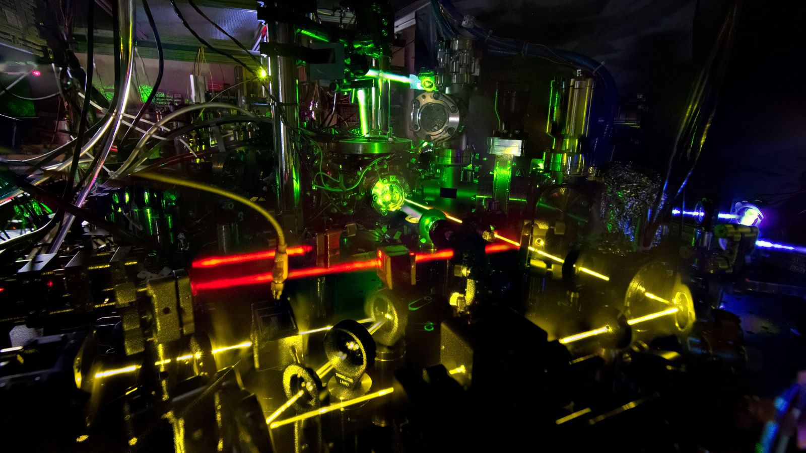
Physicists have created atomic clocks so precise that they can measure deformations in spacetime itself, according to new research.
We don’t all experience time passing equally—time passes more slowly closer to something massive’s gravitational pull, as famously theorized by Albert Einstein. And since gravity is typically interpreted as the way mass warps space itself, that means a precise-enough atomic clock could serve as a scientific tool for measuring how objects change the shape of their surrounding space.


NSW university has set up a Quantum Computer Company
Silicon Quantum Computing Pty. Ltd. (SQC) is working to create and commercialize a quantum computer based on world-leading intellectual property acquired from the Australian Centre of Excellence for Quantum Computation and Communication Technology (CQC2T). We have set ourselves a bold ambition: to develop a 10-qubit quantum integrated circuit prototype in silicon by 2022.

PANC-1 human pancreatic cancer cells are characterized by their ability to proliferate aggressively under hypovascular and hypoxic conditions in the tumor microenvironment, displaying a remarkable tolerance to nutrition starvation. The antiausterity strategy is a new approach in anticancer drug discovery aiming at the identification of potent agents that inhibit preferentially the survival of tumor cells during a limited supply of nutrients and oxygen. The new 5,8′-coupled naphthyldihydroisoquinoline alkaloid ancistrolikokine E3 (4), isolated from the Congolese liana Ancistrocladus likoko, showed potent preferential cytotoxicity against PANC-1 cells under nutrient-deprived conditions, with a PC50 value of 2.5 μM, without exhibiting toxicity in normal, nutrient-rich medium. The compound was found to induce dramatic alterations in cell morphology, leading to cell death. Moreover, it inhibited significantly PANC-1 cell migration and colony formation in a concentration-dependent manner. This study on 4 provides the first live evidence of the effect of a naphthyldihydroisoquinoline alkaloid against PANC-1 cells in nutrient-deprived medium. Mechanistic investigations conducted suggest that compound 4 is a potent inhibitor of the activation of the Akt/mTOR pathway. Furthermore, it inhibited the expression levels of the key autophagy regulators Atg5, Atg12, Beclin-1, LC3-I, and LC3-II. The results demonstrated that ancistrolikokine E3 (4) is a potent early-stage inhibitor of the autophagy pathway in PANC-1 human pancreatic cancer cells. Ancistrolikokine E3 (4) and related naphthylisoquinoline alkaloids are promising potential lead compounds for anticancer drug development based on the antiausterity strategy.
The success of SpaceX Falcon Heavy on its first launch was not just luck. Although this will be confirmed in 2019 and 2020 based upon what happens with about five planned Falcon Heavy launches.
Before the Falcon Heavy flight Musk predicted a 50 percent to 70 percent chance of success because of concerns over the difficulty predicting how the vehicle would respond to extreme aerodynamic stresses and vibrations from the clustered engines.
SpaceX has a 96.88% launch success rate (62 out of 64) with the Falcon 9. This launch success is with five major design changes for the Falcon 9 rocket.
Blue Origin has provided additional details relating to its New Glenn rocket this week via the release of its Payload User Guide that is designed to aid customers interested in launching their payloads on their launch vehicle with requirements and capabilities. Meanwhile, work is continuing on the company’s Cape Canaveral launch site and the refit of its booster landing ship.
Blue Origin is quietly preparing to head into the orbital launch market with its New Glenn rocket, named after the first American to orbit the Earth, John Glenn.
With its first rocket, New Shepard, closing in on the end of its test series, Blue’s initial focus has been towards the launch of paying customers – and onboard payloads – via its suborbital system.