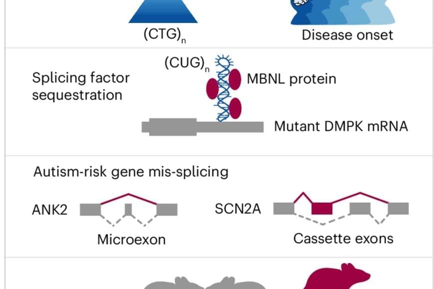
A recent discovery of a molecular connection between autism and myotonic dystrophy, a type of neuromuscular disease, may provide a breakthrough on how clinicians approach autism spectrum disorder.
The new study by an interdisciplinary team of biomedical scientists, published in Nature Neuroscience, used myotonic dystrophy as a tool or model to learn more about autism – effectively using one disorder to better understand the other.
“We identified a new pathway that can lead to autism,” said the research lead. “We found that a genetic mutation in a certain gene can disrupt the expression of multiple autism-related genes during brain development, causing autism.”
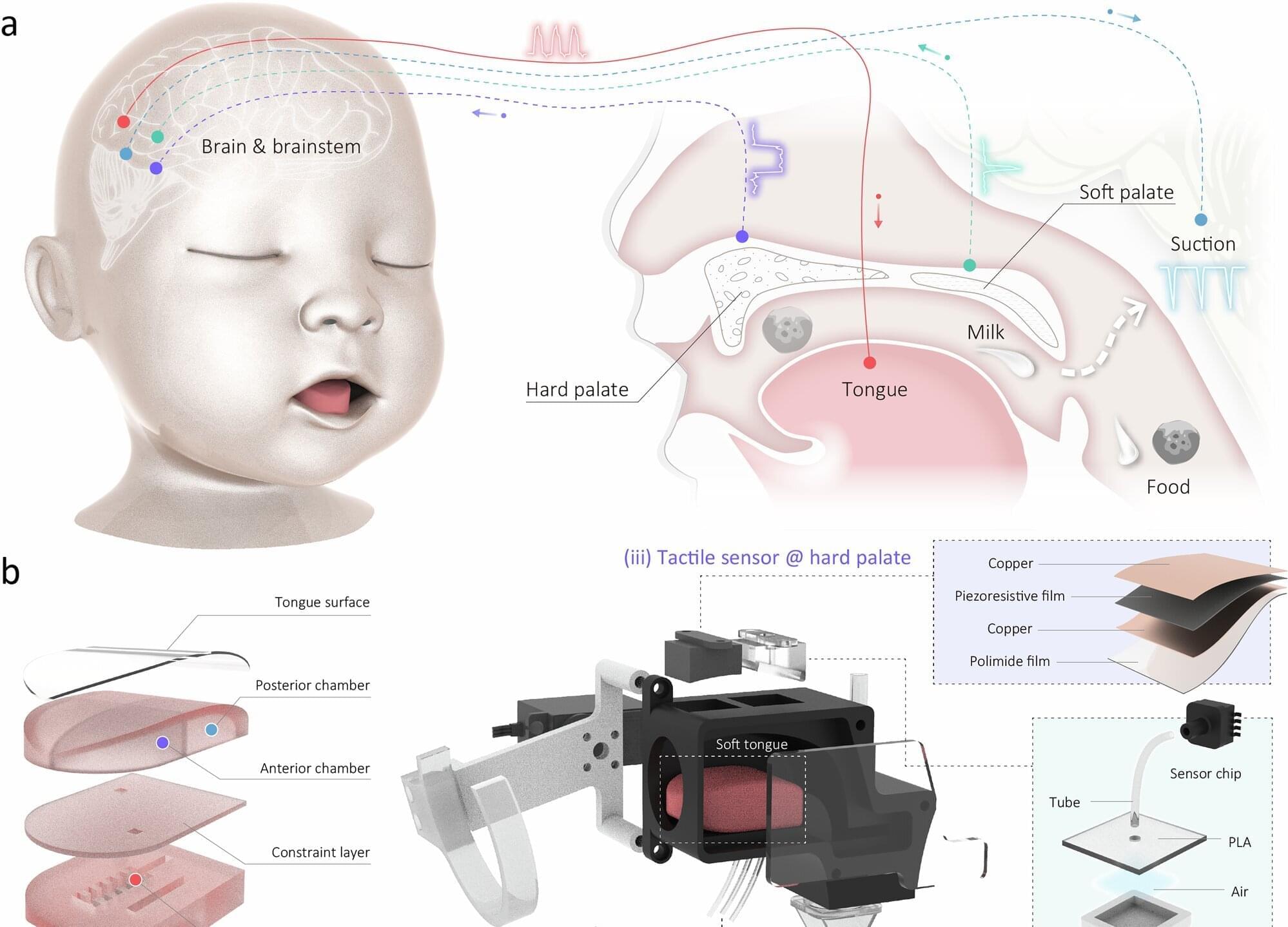
A combined team of roboticists from CREATE Lab, EPFL and Nestlé Research Lausanne, both in Switzerland, has developed a soft robot that was designed to mimic human infant motor development and the way infants feed.
In their paper published in the journal npj Robotics, the group describes how they used a variety of techniques to give their robot the ability to simulate the way human infants feed, from birth until approximately six months old.
Prior research has shown that it is difficult to develop invasive medical procedures for infants and babies due to the lack of usable test subjects. Methods currently in use, such as simulations, observational instruments and imaging tend to fall short due to their differences compared to real human infants. To overcome such problems, the team in Switzerland has designed, built, and tested a soft robotic infant that can be used for such purposes.
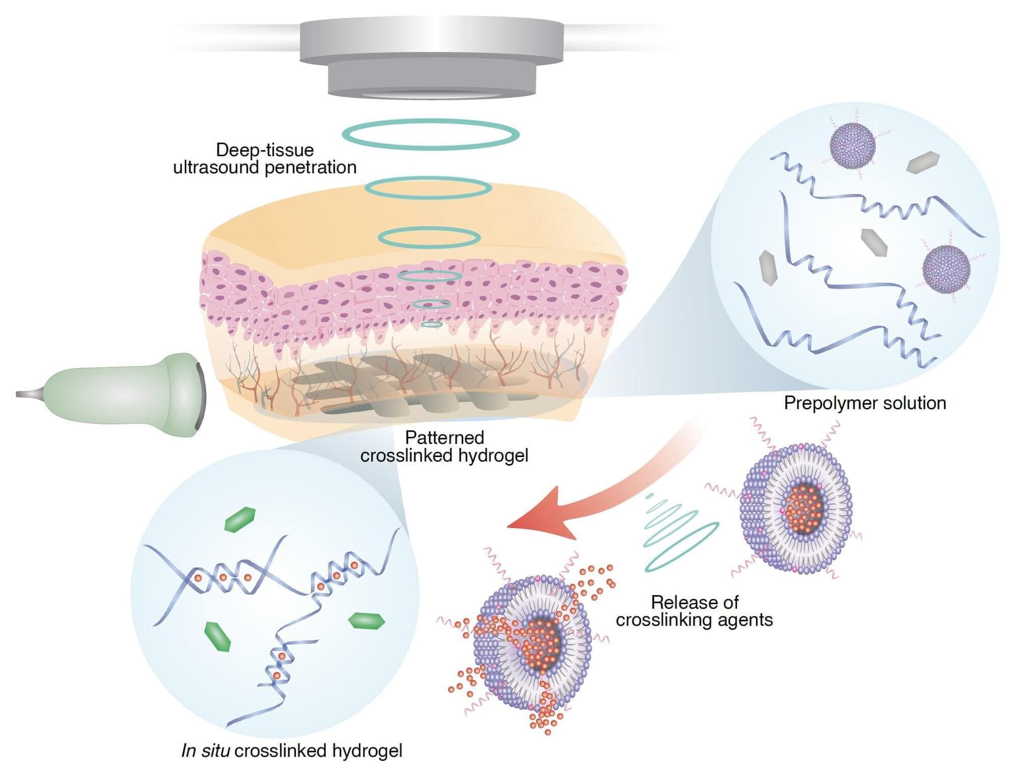
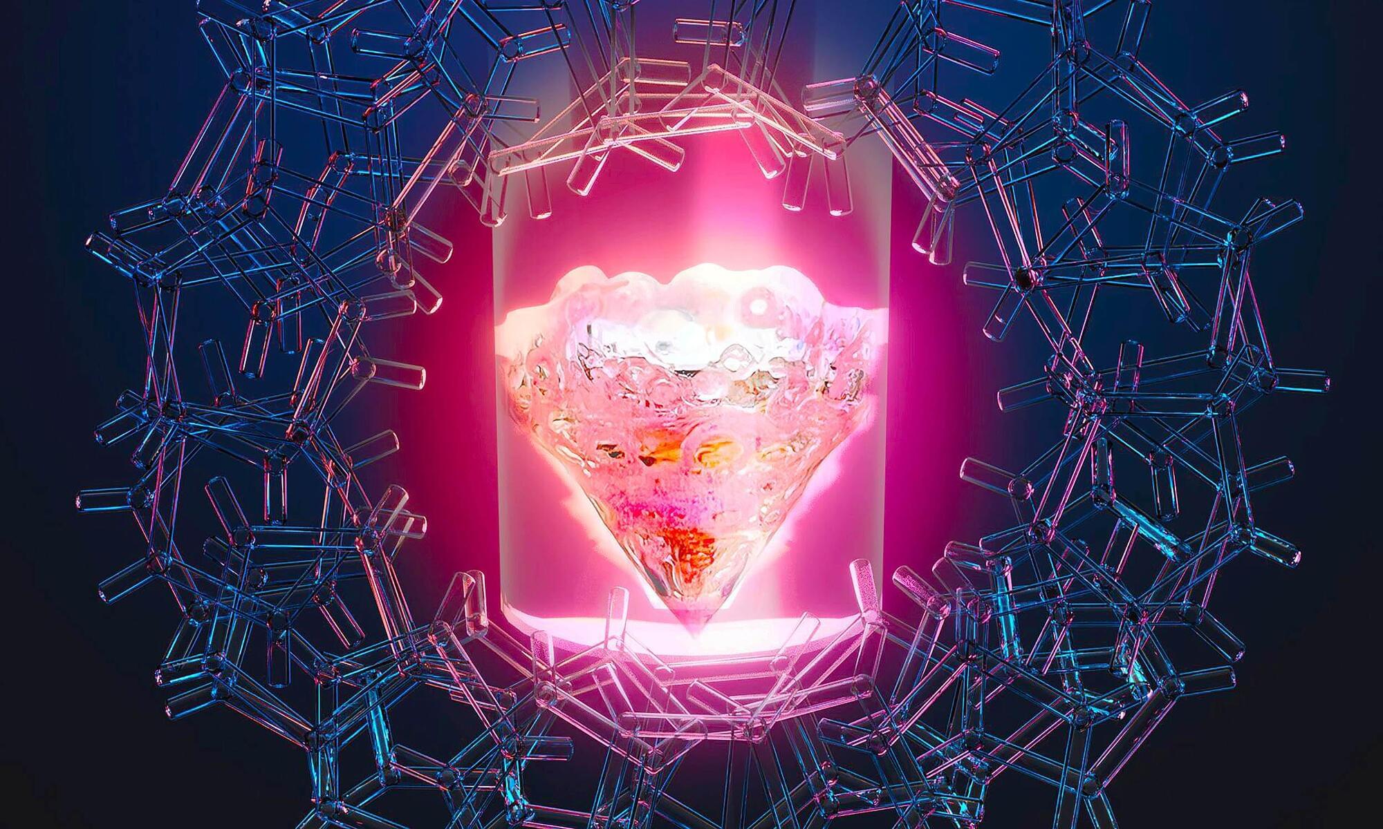
Imagine that doctors could precisely print miniature capsules capable of delivering cells needed for tissue repair exactly where they are needed inside a beating heart.
A team of scientists led by Caltech has taken a significant step toward that ultimate goal, having developed a method for 3D-printing polymers at specific locations deep within living animals. The technique relies on sound for localization and has already been used to print polymer capsules for selective drug delivery as well as glue-like polymers to seal internal wounds.
Previously, scientists have used infrared light to trigger polymerization, the linking of the basic units, or monomers, of polymers within living animals.
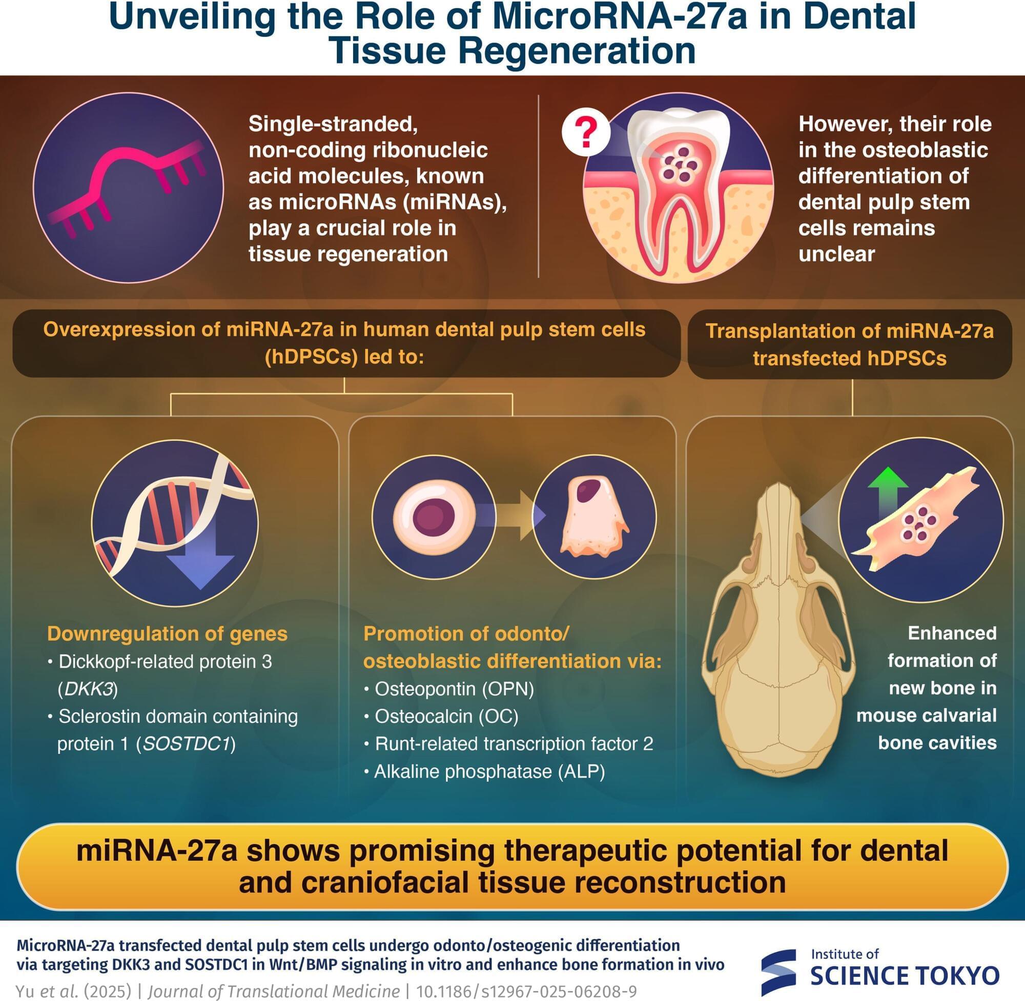
Dental caries (tooth decay) is a common oral health condition that often causes significant pain and discomfort and may even lead to tooth loss. In severe and untreated cases, bacterial infection combined with the host’s immune response can cause bone resorption, or the breakdown of bone tissue in the tooth root. Moreover, traditional treatments for advanced dental caries, such as surgery, can result in bone defects that require complex bone grafting procedures.
Building on this knowledge, bone tissue engineering and dental tissue regeneration have gained the attention of researchers worldwide. Recent reports suggest that microRNAs (miRNAs)—small, non-coding ribonucleic acid sequences—play a key role in bone tissue regeneration. However, the underlying mechanisms and pathways regulated by miRNAs remain unclear.
To investigate the intrinsic processes involved in dental bone repair, a team of researchers led by Associate Professor Nobuyuki Kawashima, graduate student Ziniu Yu, and Professor Takashi Okiji from the Graduate School of Medical and Dental Sciences, Institute of Science Tokyo (Science Tokyo), Japan, has conducted a series of innovative experiments using human dental pulp stem cells (hDPSCs) and mice.
Meridian Magazine positions itself as a publication for members of The Church of Jesus Christ of Latter-day Saints, the largest Mormon denomination. I don’t know much about Meridian or the people behind it. But today I learned that they’re willing to publish a fear-mongering distortion of Transhumanism, “Human 2.0 Is Here — And You Didn’t Even Notice” by Alexis Tarkaleson. Despite their positioning, I wish to make make clear that such behavior is not aligned with the values that the Church advocates.
Tarkaleson says “mind uploading” is an outlandish tale. What’s her take on tales of transfiguration and resurrection? Are those equally outlandish? Surely she’s aware that those doctrines require the possibility of mind (or spirit body) moving from one physical body to another, consistent with hypotheses of mind uploading.
How about cryonics, yet another outlandish tale she identifies? I’m curious to know what she thinks about the Church’s advocacy to collect genealogy and preserve family history, with intent to facilitate redemption of the dead. And what about proxy rituals that we perform for the dead? Most of the world probably thinks the Church’s practices in these areas are at least as outlandish as those of cryonicists.
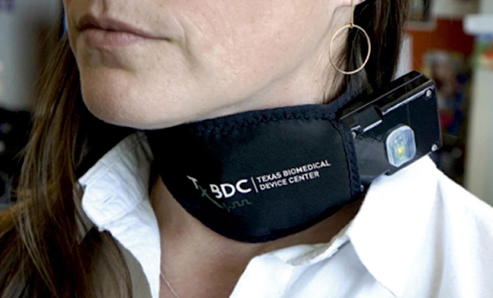
Groundbreaking research has revealed a new method of potentially eliminating hard-to-treat post-traumatic stress disorder (PTSD) diagnoses in patients by employing a novel kind of therapy: stimulation of the vagus nerve.
The new treatment offers new hope for those long afflicted by PTSD diagnoses that have traditionally proven to be resistant to conventional treatment methods.
Scientists from the University of Texas at Dallas (UTD) and Baylor University Medical Center conducted the research, discovering that participants were symptom-free for up to six months after completing the experimental therapy.
What happens when AI starts improving itself without human input? Self-improving AI agents are evolving faster than anyone predicted—rewriting their own code, learning from mistakes, and inching closer to surpassing giants like OpenAI. This isn’t science fiction; it’s the AI singularity’s opening act, and the stakes couldn’t be higher.
How do self-improving agents work? Unlike static models such as GPT-4, these systems use recursive self-improvement—analyzing their flaws, generating smarter algorithms, and iterating endlessly. Projects like AutoGPT and BabyAGI already demonstrate eerie autonomy, from debugging code to launching micro-businesses. We’ll dissect their architecture and compare them to OpenAI’s human-dependent models. Spoiler: The gap is narrowing fast.
Why is OpenAI sweating? While OpenAI focuses on safety and scalability, self-improving agents prioritize raw, exponential growth. Imagine an AI that optimizes itself 24/7, mastering quantum computing over a weekend or cracking protein folding in hours. But there’s a dark side: no “off switch,” biased self-modifications, and the risk of uncontrolled superintelligence.
Who will dominate the AI race? We’ll explore leaked research, ethical debates, and the critical question: Can OpenAI’s cautious approach outpace agents that learn to outthink their creators? Like, subscribe, and hit the bell—the future of AI is rewriting itself.
Can self-improving AI surpass OpenAI? What are autonomous AI agents? How dangerous is recursive AI? Will AI become uncontrollable? Can we stop self-improving AI? This video exposes the truth. Watch now—before the machines outpace us.