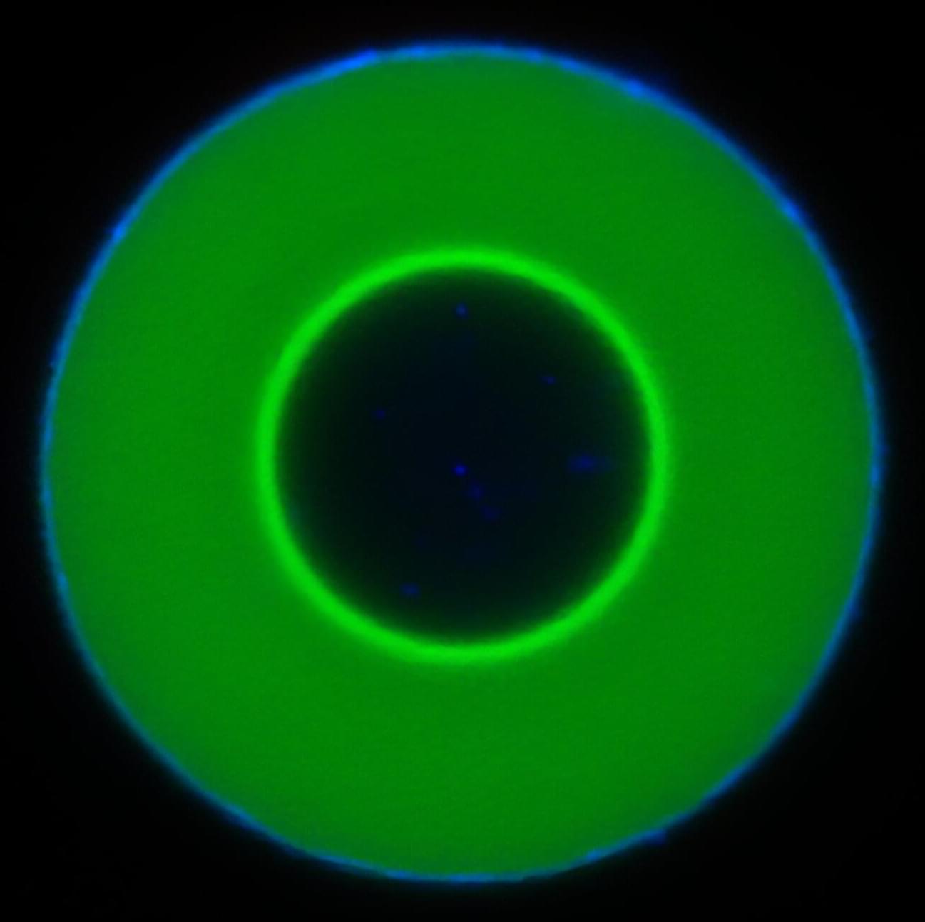
Toggle light / dark theme

Discussions are emerging about conducting clinical trials on humans with nanorobots for medical applications. Currently, in the United States, four burgeoning companies are striving towards this aim, working to advance their nanomachines into Phase 1 studies, subsequent to laboratory research and preclinical trials on animals.

The article “Delivering drugs with microrobots”, published in Science on December 7, 2023, has recaptured the international scientific community’s attention on the practical, effective use of nanorobots in Clinical Practice and Medicine.

Its author, Bradley Nelson, a Robotics and Intelligent Systems professor at ETH Zurich, poses a straightforward question: where are these diminutive biocompatible machines, designed to be injected into the human body for more efficient exploration, internal repair, and precise, targeted drug delivery? Researchers have discussed them for years – he notes – yet we still do not see them progressing from laboratories to the forefront of clinical trials. How close are we to this milestone?

Longstanding challenges in biomedical research such as monitoring brain chemistry and tracking the spread of drugs through the body require much smaller and more precise sensors. A new nanoscale sensor that can monitor areas 1,000 times smaller than current technology and can track subtle changes in the chemical content of biological tissue with sub-second resolution, greatly outperforming standard technologies.

The device, developed by researchers at the University of Illinois Urbana-Champaign, is silicon-based and takes advantage of techniques developed for microelectronics manufacturing. The small device size enables it to collect chemical content with close to 100% efficiency from highly localized regions of in a fraction of a second. The capabilities of this new nanodialysis device are reported in the journal ACS Nano.

“With our nanodialysis device, we take an established technique and push it into a new extreme, making problems that were impossible before quite feasible now,” said Yurii Vlasov, a U. of I. electrical & computer engineering professor and a co-lead of the study. “Moreover, since our devices are made on silicon using microelectronics fabrication techniques, they can be manufactured and deployed on large scales.”

Relying on sub-wavelength nanostructures, metasurfaces have been shown as promising candidates for replacing conventional free-space optical components by arbitrarily manipulating the amplitude, phase, and polarization of optical wavefronts in certain applications1,2,3. In recent years, the scope of their applications has been expanded towards complete spatio-temporal control through the introduction of active metasurfaces. These developments open up exciting new possibilities for dynamic holography4, faster spatial light modulators5, and fast optical beam steering for LiDAR6. Large efforts have been channeled into various modulation mechanisms7. Microelectromechanical and nanoelectromechanical systems (MEMS and NEMS)8,9,10,11 have the advantages of low-cost and CMOS-compatibility, but the speed is limited up to MHz. Phase-change materials12,13,14 have fast, drastic, and non-volatile refractive index change, but lack continuous refractive index tuning and have a limited number of cycles constraining applicability to reconfigurable devices. Through molecule reorientation, liquid crystal can have index modulation over 10%, while under relatively low applied voltages Tunable liquid crystal metasurfaces, U.S. patent number 10,665,953 [Application Number 16/505,687]15. Techniques of liquid crystal integration have also advanced after decades of development. However, the tuning speeds are limited to kHz range16. Thermal-optic effects can induce relatively large refractive index changes17,18, but the speed is inherently limited and the on-chip thermal management can be challenging. The co-integration of transparent conductive oxide and metallic plasmonic structures5,6 has been demonstrated in epsilon-near-zero (ENZ) regime to control the wavefront of reflected light, but the low reflection amplitude induced by the optical loss of the materials and the ENZ regime is unavoidable.

In modern photonics, a multitude of technologies for tunable optics and frequency conversion19,20 are realized with nonlinear materials that have low loss and a strong χ effect, such as lithium niobate21,22, aluminum nitride23, and organic electro-optic (OEO) materials24. Their ultrafast responses make it possible to use RF or millimeter-wave control25. Developments in computational chemistry have also led to artificially engineered organic molecules that have record-high nonlinear coefficients with long-term and high-temperature stability26,27. However, their potential in modifying free-space light has been relatively unexplored until recently. Several OEO material-hybrid designs have demonstrated improved tunability of metasurfaces28,29,30. Utilizing dielectric resonant structures and RF-compatible coplanar waveguides, a free-space silicon-organic modulator has recently accomplished GHz modulation speed31. However, all demonstrations to date require high operating voltages ± 60V, due to low resonance tuning capability (frequency shift / voltage), which hinders their integration with electronic chips.

In this work, we propose combining high-Q metasurfaces based on slot-mode resonances with the unique nano-fabrication techniques enabled by OEO materials, which drastically reduces the operating voltage. The low voltage is mainly achieved from the ability to place the electrodes in close proximity to each other while hosting high-Q modes in between and the large overlap of the optical and RF fields in OEO materials. In the following sections, we first provide the design concepts and considerations for achieving a reduced operating voltage. Next, we numerically demonstrate the advantage of a particular selected mode compared to other supported modes in the structure. Finally, we experimentally realize our concepts and characterize the performance of the electro-optic metasurface.

National University of Singapore researchers and their collaborators have unveiled a novel concept termed “supercritical coupling” that enables a several-fold increase in photon upconversion efficiency. This discovery not only challenges existing paradigms, but also opens a new direction in the control of light emission.

Photon upconversion, the process of converting low-energy photons into higher-energy ones, is a crucial technique with broad applications, ranging from super-resolution imaging to advanced photonic devices. Despite considerable progress, the quest for efficient upconversion has faced challenges due to inherent limitations in the irradiance of lanthanide-doped nanoparticles and the critical coupling conditions of optical resonances.

The concept of “supercritical coupling” plays a pivotal role in addressing these challenges. This fundamentally new approach, proposed by a research team led by Professor Liu Xiaogang from the Department of Chemistry, NUS and his collaborator, Dr. Gianluigi Zito from the National Research Council of Italy leverages on the physics of “bound states in the continuum” (BICs).

The U.S. Naval Research Laboratory (NRL), working together with Kansas State University, has announced the discovery of slab waveguides made from the two-dimensional material hexagonal boron nitride. This milestone has been documented in the journal Advanced Materials.

Two-dimensional (2D) materials are a class of materials that can be reduced to the monolayer limit by mechanically peeling the layers apart. The weak interlayer attractions, or van der Waals attraction, allows the layers to be separated via the so-called “Scotch tape” method. The most famous 2D material, graphene, is a semimetallic material consisting of a single layer of carbon atoms. Recently, other 2D materials including semiconducting transition metal dichalcogenides (TMDs) and insulating hexagonal boron nitride (hBN) have also garnered attention. When reduced near the monolayer limit, 2D materials have unique nanoscale properties that are appealing for creating atomically thin electronic and optical devices.

Recently, a research team from Pohang University of Science and Technology (POSTECH) has employed metasurfaces to fabricate angle-dependent holograms with multiple functions. This technology allows holograms to display multiple images based on the observer’s viewing angle. The findings were published in Nano Letters.

Objects can appear distinct depending on the viewer’s position, a concept that can be harnessed in to generate cinematic and realistic 3D holograms presenting different images based on the viewing angle. However, the current challenge lies in controlling light dispersion according to the angle, making the application of nano-optics in this context a complex endeavor.

The team addressed this challenge by leveraging metasurfaces, artificial nanostructures capable of precisely manipulating the characteristics of light. These metasurfaces are incredibly thin and lightweight, approximately one-hundredth the thickness of a human hair, making them promising for applications in miniaturized displays such as virtual and augmented reality devices.

Imagine an army of self-propelling, radioisotope-covered particles 2,500 to 10,000 times smaller than a speck of dust that, upon injection into the body, search for and attach themselves to cancerous tumours, destroying them. Sounds like science fiction? Not so for mice with bladder cancer.

Researchers in Spain report that nanoparticles containing radioactive iodine and which propel themselves upon reaction with urea have the ability to distinguish cancerous bladder tumours from healthy tissue. These “nanobots” penetrate the tumour’s extracellular matrix and accumulate within it, enabling the radionuclide therapy to reach its precise target. In a study conducted at the Institute for Bioengineering of Catalonia (IBEC) in Barcelona, mice receiving a single dose of this treatment had a 90% reduction in the size of bladder tumours compared with untreated animals.

This novel approach may one day revolutionize the treatment of bladder cancer. Bladder cancer is the tenth most common cancer in the world, with over 600,000 new cases diagnosed in 2022 and more than 220,000 deaths globally, according to the World Health Organization’s Global Cancer Observatory.

Researchers at Osaka University have developed a groundbreaking flexible optical sensor that works even when crumpled. Using carbon nanotube photodetectors and wireless Bluetooth technology, this sensor enables non-invasive analysis and holds promise for advancements in imaging, wearable technology, and soft robotics. Credit: SciTechDaily.com.

Researchers at Osaka University have created a soft, pliable, and wireless optical sensor using carbon nanotubes and organic transistors on an ultra-thin polymer film. This innovation is poised to open new possibilities in imaging technologies and non-destructive analysis techniques.

Recent years have brought remarkable progress in imaging technology, ranging from high-speed optical sensors capable of capturing more than two million frames per second to compact, lensless cameras that can capture images with just a single pixel.

Canadian researchers led by Montreal radiologist Gilles Soulez have developed a novel approach to treat liver tumors using magnet-guided microrobots in an MRI device.

The idea of injecting microscopic robots into the bloodstream to heal the human body is not new. It’s also not science fiction. Guided by an , miniature biocompatible robots, made of magnetizable iron oxide nanoparticles, can theoretically provide in a very targeted manner.

Until now, there has been a technical obstacle: the force of gravity of these microrobots exceeds that of the magnetic force, which limits their guidance when the tumor is located higher than the injection site. While the magnetic field of the MRI is high, the magnetic gradients used for navigation and to generate MRI images are weaker.