Researchers have advanced smart coatings by manipulating nanoparticles to reconfigure themselves by using microscopy and computer simulation.
Researchers have advanced smart coatings by manipulating nanoparticles to reconfigure themselves by using microscopy and computer simulation.
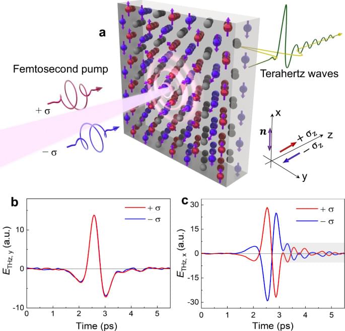
Antiferromagnets are promising for nano-oscillator in terahertz frequency. However, realizing antiferromagnetic moment oscillation via spin-orbit torque remains elusive. Here, the authors demonstrate oscillations in Mn2Au films.
Scientists at the Fritz Haber Institute of the Max Planck Society have developed a revolutionary microscopy method that enables the direct visualization of nanostructures and their optical properties.
This breakthrough allows researchers to observe nanoscale materials, like metamaterials, in unprecedented detail by manipulating light in innovative ways. The method has taken over five years to develop and leverages the unique capabilities of the Free Electron Laser. The implications of this research are vast, offering the potential to advance flat optics, shrink 3D optics to 2D, and create more efficient optical devices.
Tailoring Light With Nanomaterials
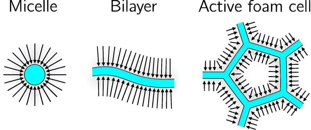
Many fundamental processes of life, and their synthetic counterparts in nanotechnology, are based on the autonomous assembly of individual particles into complex patterns. LMU physicist Professor Erwin Frey, Chair of Statistical and Biological Physics at LMU Munich and member of the ORIGINS Excellence Cluster, investigates the fundamental principles of this self-organization.
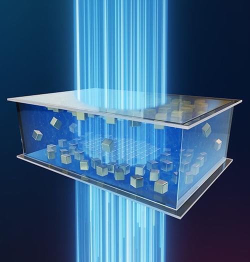
A view into how nanoscale building blocks can rearrange into different organized structures on command is now possible with an approach that combines an electron microscope, a small sample holder with microscopic channels, and computer simulations, according to a new study by researchers at the University of Michigan and Indiana University.
The approach could eventually enable smart materials and coatings that can switch between different optical, mechanical and electronic properties.
“One of my favorite examples of this phenomenon in nature is in chameleons,” said Tobias Dwyer, U-M doctoral student in chemical engineering and co-first author of the study published in Nature Chemical Engineering (“Engineering and direct imaging of nanocube self-assembly pathways”). “Chameleons change color by altering the spacing between nanocrystals in their skin. The dream is to design a dynamic and multifunctional system that can be as good as some of the examples that we see in biology.”
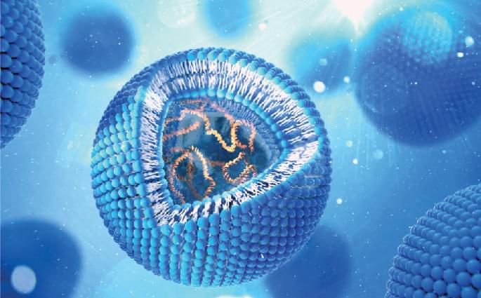
The 2024 Kavli Prize in Nanoscience is awarded to three nanomedicine pioneers who laid the foundation of controlled release, biomedical imaging and diagnostics.
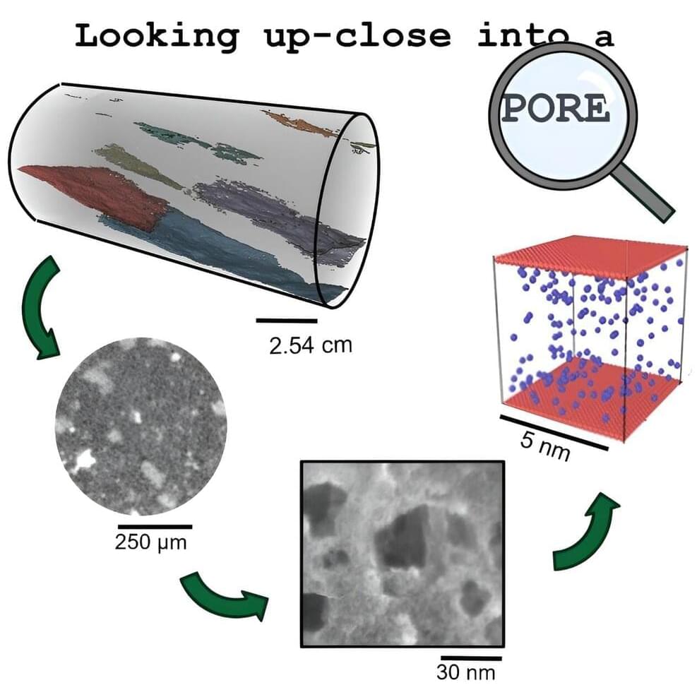
A team of researchers is working on a multidisciplinary approach to advancing the exploration of shale rock as a suitable geological seal for resource recovery and underground storage. Given that the pore space in shale rock is predominantly sub-micron, these studies focus on the micro and the nanoscale.
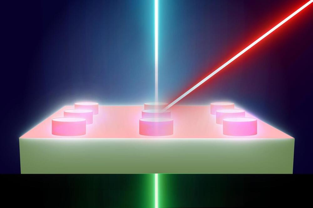
Scientists from the Department of Physical Chemistry at the Fritz Haber Institute have made an innovative discovery in nanoscale optoelectronics, as detailed in their recent publication in Nature Communications (“Atomic-Precision Control of Plasmon-Induced Single-Molecule Switching in a Metal–Semiconductor Nanojunction”).
The study introduced a groundbreaking method for achieving unprecedented control over single-molecule photoswitching. This breakthrough could transform the future of nanodevice technology.
Schematic view of the plasmon-driven switching of a single PTCDA molecule. (Image: Fritz Haber Institute)
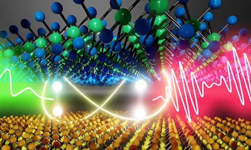
Quantum technology relies on qubits, the fundamental units of quantum computers, whose operation is influenced by quantum coherence time. Scientists believe that moiré excitons — electron-hole pairs trapped in overlapping moiré interference fringes — could serve as qubits in future nano-semiconductors. However, previous limitations in focusing light have caused optical interference, making it difficult to measure these excitons accurately.
Kyoto University researchers have developed a new technique to reduce moiré excitons, allowing for accurate measurement of quantum coherence time. Their findings, published in Nature Communications, reveal that the quantum coherence of a single moiré exciton remains stable for over 12 picoseconds at −269°C, significantly longer than that of excitons in traditional two-dimensional semiconductors. The confined moiré excitons in interference fringes help maintain quantum coherence, advancing the potential of quantum technology.
“We combined electron beam microfabrication techniques with reactive ion etching. By utilizing Michelson interferometry on the emission signal from a single moiré exciton, we could directly measure its quantum coherence time,” said Kazunari Matsuda of KyotoU’s Institute Advanced Energy.
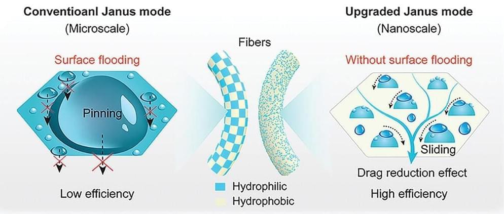
Researchers develop fibers with nanoscale surface modifications that significantly improve fog water collection rates, offering a promising solution for freshwater scarcity.