Artificial camouflage is the functional mimicry of the natural camouflage that can be observed in a wide range of species1,2,3. Especially, since the 1800s, there were a lot of interesting studies on camouflage technology for military purposes which increases survivability and identification of an anonymous object as belonging to a specific military force4,5. Along with previous studies on camouflage technology and natural camouflage, artificial camouflage is becoming an important subject for recently evolving technologies such as advanced soft robotics1,6,7,8 electronic skin in particular9,10,11,12. Background matching and disruptive coloration are generally claimed to be the underlying principles of camouflage covering many detailed subprinciples13, and these necessitate not only simple coloration but also a selective expression of various disruptive patterns according to the background. While the active camouflage found in nature mostly relies on the mechanical action of the muscle cells14,15,16, artificial camouflage is free from matching the actual anatomies of the color-changing animals and therefore incorporates much more diverse strategies17,18,19,20,21,22, but the dominant technology for the practical artificial camouflage at visible regime (400–700 nm wavelength), especially RGB domain, is not fully established so far. Since the most familiar and direct camouflage strategy is to exhibit a similar color to the background23,24,25, a prerequisite of an artificial camouflage at a unit device level is to convey a wide range of the visible spectrum that can be controlled and changed as occasion demands26,27,28. At the same time, the corresponding unit should be flexible and mechanically robust, especially for wearable purposes, to easily cover the target body as attachable patches without interrupting the internal structures, while being compatible with the ambient conditions and the associated movements of the wearer29,30.
System integration of the unit device into a complete artificial camouflage device, on the other hand, brings several additional issues to consider apart from the preceding requirements. Firstly, the complexity of the unit device is anticipated to be increased as the sensor and the control circuit, which are required for the autonomous retrieval and implementation of the adjacent color, are integrated into a multiplexed configuration. Simultaneously, for nontrivial body size, the concealment will be no longer effective with a single unit unless the background consists of a monotone. As a simple solution to this problem, unit devices are often laterally pixelated12,18 to achieve spatial variation in the coloration. Since its resolution is determined by the numbers of the pixelated units and their sizes, the conception of a high-resolution artificial camouflage device that incorporates densely packed arrays of individually addressable multiplexed units leads to an explosive increase in the system complexity. While on the other hand, solely from the perspective of camouflage performance, the delivery of high spatial frequency information is important for more natural concealment by articulating the texture and the patterns of the surface to mimic the microhabitats of the living environments31,32. As a result, the development of autonomous and adaptive artificial camouflage at a complete device level with natural camouflage characteristics becomes an exceptionally challenging task.
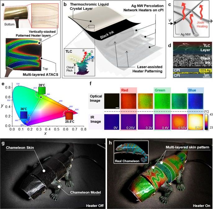
Our strategy is to combine thermochromic liquid crystal (TLC) ink with the vertically stacked multilayer silver (Ag) nanowire (NW) heaters to tackle the obstacles raised from the earlier concept and develop more practical, scalable, and high-performance artificial camouflage at a complete device level. The tunable coloration of TLC, whose reflective spectrum can be controlled over a wide range of the visible spectrum within the narrow range of temperature33,34, has been acknowledged as a potential candidate for artificial camouflage applications before21,34, but its usage has been more focused on temperature measurement35,36,37,38 owing to its high sensitivity to the temperature change. The susceptible response towards temperature is indeed an unfavorable feature for the thermal stability against changes in the external environment, but also enables compact input range and low power consumption during the operation once the temperature is accurately controlled.

