Antoine Galand, Director of Technology, GraphWear
Nanotechnology was once the stuff of science fiction, but today the concept of creating devices and machines that are several thousand times smaller than the width of a human hair is a well-established fact. The rise of nanotechnology has already transformed industries ranging from consumer electronics to textile manufacturing and cosmetics by unlocking new materials and processes at the nanoscale. The device you’re reading this on, for example, is only possible because of techniques adopted in the semiconductor industry that enable us to pattern silicon and metals to create the microscopic circuits and switches that are at the heart of modern computers.
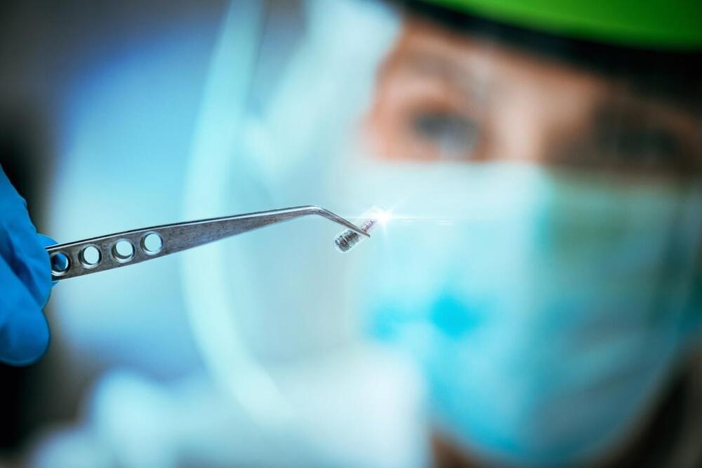
One of the most promising applications of our newfound ability to manipulate individual atoms and molecules is in healthcare, where the ability of doctors to treat disease has been hamstrung by relatively blunt “macro” solutions. The human body is a remarkably complex system where, fundamentally, nanoscale processes occurring inside cells are what determine whether we are sick or healthy. If we’re ever going to cure diseases like diabetes, cancer or Alzheimer’s, we need technologies that work at their scale. Although medical nanotechnologies are relatively new, they’re already impacting the way we diagnose, treat and prevent a broad range of diseases.