Menu

Blog

Archive for the ‘nanotechnology’ category: Page 202

Feb 23, 2017

Lanthanide-Doped KLu2F7 Nanoparticles with High Upconversion Luminescence Performance: A Comparative Study

Posted by in categories: energy, nanotechnology

Nice find on nanoparticles and energy transfer — important in scalable devices, energy conservation, etc.


The development, design and the performance evaluation of rare-earth doped host materials is important for further optical investigation and industrial applications. Herein, we successfully fabricate KLu2F7 upconversion nanoparticles (UCNPs) through hydrothermal synthesis by controlling the fluorine-to-lanthanide-ion molar ratio. The structural and morphological results show that the samples are orthorhombic-phase hexagonal-prisms UCNPs, with average side length of 80 nm and average thickness of 110 nm. The reaction time dependent crystal growth experiment suggests that the phase transformation is a thermo-dynamical process and the increasing F/Ln3+ ratio favors the formation of the thermo-dynamical stable phase — orthorhombic KLu2F7 structure. The upconversion luminescence (UCL) spectra display that the orthorhombic KLu2F7:Yb/Er UCNPs present stronger UCL as much as 280-fold than their cubic counterparts. The UCNPS also display better UCL performance compared with the popular hexagonal-phase NaREF4 (RE = Y, Gd). Our mechanistic investigation, including Judd-Ofelt analysis and time decay behaviors, suggests that the lanthanide tetrad clusters structure at sublattice level accounts for the saturated luminescence and highly efficient UCL in KLu2F7:Yb/Er UCNPs. Our research demonstrates that the orthorhombic KLu2F7 is a promising host material for UCL and can find potential applications in lasing, photovoltaics and biolabeling techniques.

Read more

Feb 23, 2017

Spiky Nanostructures Capture Life’s Fine Details

Posted by in categories: biotech/medical, nanotechnology

A new day for imaging.


Optical microscopes that use lenses to bounce photons off objects have trouble distinguishing nanometer-scale objects smaller than the imaging beam’s wavelength, such as proteins and DNA. An innovative ‘hyperlens’ designed at A* STAR can overcome optical diffraction limits by capturing high-resolution information held by short-lived or evanescent waves lurking near a target’s surface.

Hyperlens devices — composed of thin stacks of alternate metal and plastic layers — have raised prospects for capturing living biological processes in action with high–speed optics. Key to their operation are oscillating electrons, known as surface plasmons, that resonate with and enhance evanescent waves that appear when photons strike a solid object. The narrow wavelengths of evanescent beams give nanoscale resolution to images when the hyperlens propagates the images to a standard microscope.

Continue reading “Spiky Nanostructures Capture Life’s Fine Details” »

Feb 23, 2017

Nano-size revolution is getting bigger

Posted by in categories: materials, nanotechnology

And, we just started. Just wait — in the next 6 to 8 months; I will some amazing news to share on QBS and BMI. smile


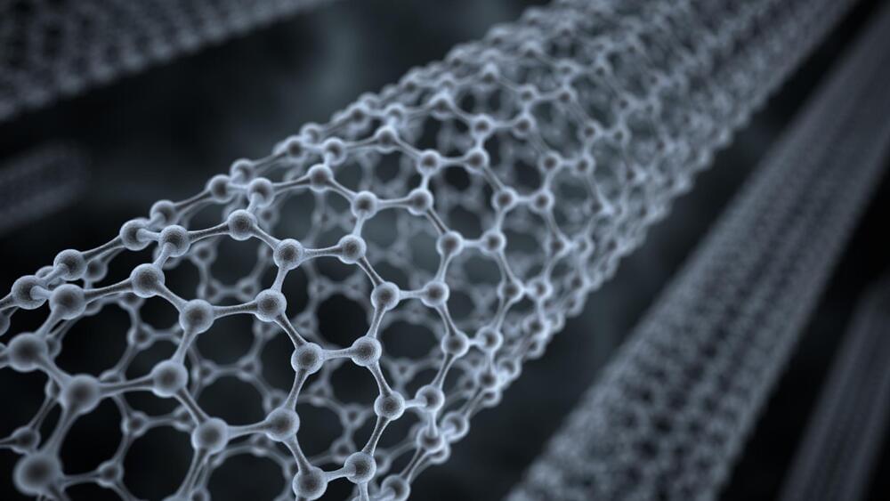
An explosion of nanotechnology research and development is occurring as newly identified forms of carbon, including graphene, carbon nanotubes and nano-diamonds, pave the way for new products and industries.

This article is sponsored by Flinders University.

Continue reading “Nano-size revolution is getting bigger” »

Feb 22, 2017

Switched-on DNA spark nano-electronic applications

Posted by in categories: bioengineering, biotech/medical, nanotechnology

DNA, the stuff of life, may very well also pack quite the jolt for engineers trying to advance the development of tiny, low-cost electronic devices.

Much like flipping your light switch at home — –only on a scale 1,000 times smaller than a human hair — –an ASU-led team has now developed the first controllable DNA switch to regulate the flow of electricity within a single, atomic-sized molecule. The new study, led by ASU Biodesign Institute researcher Nongjian Tao, was published in the advanced online journal Nature Communications ( DOI: 10.1038/ncomms14471).

“It has been established that charge transport is possible in DNA, but for a useful device, one wants to be able to turn the charge transport on and off. We achieved this goal by chemically modifying DNA,” said Tao, who directs the Biodesign Center for Bioelectronics and Biosensors and is a professor in the Fulton Schools of Engineering.

Continue reading “Switched-on DNA spark nano-electronic applications” »

Feb 22, 2017

Scientists create a nano-trampoline to probe quantum behavior

Posted by in categories: nanotechnology, quantum physics

Very cool.


A research group from Bar-Ilan University, in collaboration with French colleagues at CNRS Grenoble, has developed a unique experiment to detect quantum events in ultra-thin films. This novel research, to be published in the scientific journal Nature Communications, enhances the understanding of basic phenomena that occur in nano-sized systems close to absolute zero temperature.

Transitions, Phases and Critical Points

Continue reading “Scientists create a nano-trampoline to probe quantum behavior” »

Feb 22, 2017

Solar photovoltaic windows rely on inexpensive silicon quantum dots

Posted by in categories: nanotechnology, quantum physics, solar power, sustainability

Luminescent solar concentrators (LSCs), which are flat panes of mostly transparent material that take sunlight (both diffuse and directed) and concentrate it at the panes’ edges, can be used as “photovoltaic windows,” which, as the name makes clear, collect solar energy while serving as ordinary windows. Now, researchers at the Università degli Studi di Milano-Bicocca and Glass to Power Srl (both of Milano, Italy) and the University of Minnesota (Minneapolis, MN) are lowering the potential cost of such windows by using silicon nanoparticles as the fluorescent absorber/emitter in the LSC windows.

Read more

Feb 21, 2017

Turning nano-antennas on the right side

Posted by in category: nanotechnology

Optical nano-antennas are ideal to enhance light-matter interactions at the nanometer scale. Yet in most designs, the region of maximum field localization and enhancement, the “hotspot”, is not readily accessible since it is buried into the nanostructure.

In a recent collaboration between EPFL in Lausanne, Fresnel Institute in Marseille and ICFO groups led by ICREA Professors at ICFO Maria Garcia-Parajo and Niek van Hulst, researchers present a new nanofabrication technique that applies planarization, etch back and template stripping to expose the excitation hotspot at the surface.

The large flat surface arrays of in-plane nano-antennas feature gaps as small as 10 nm with sharp edges, excellent reproducibility and full surface accessibility of the hotspot confined region. The novel fabrication approach drastically improves the optical performance of plasmonic nano-antennas to yield giant fluorescence enhancement factors, together with nanoscale detection volumes in the 20 zepto-liter range.

Read more

Feb 21, 2017

Photon Gun Could Further Development of Photonic Quantum Network

Posted by in categories: nanotechnology, quantum physics

A photonic nanostructure for constructing quantum photonic circuits for quantum networks has been developed, which could impact the optics and photoni.

Read more

Feb 16, 2017

Company Claims Brain Transplants Could Bring Back the Dead by 2045

Posted by in categories: biotech/medical, cyborgs, life extension, military, nanotechnology, neuroscience, Ray Kurzweil, robotics/AI, singularity

Not too shock by this given other transplant patient’s stories of memories, etc.


1 brains
There are a lot of outrageous claims being made within the halls of neuroscience and artificial intelligence. Whether exaggerations, wishful thinking, the dreams of the egocentric and megalomaniacal to be immortal, or just drumming up funding for a never-ending round of “scientific investigation,” the year 2045 seems to always be cited as a target date.

Continue reading “Company Claims Brain Transplants Could Bring Back the Dead by 2045” »

Feb 16, 2017

From Initial Nucleation to Cassie-Baxter State of Condensed Droplets on Nanotextured Superhydrophobic Surfaces

Posted by in categories: energy, nanotechnology

Science mimicking nature’s dew in a lab. Important btw in how we looking at H2O harvesting and improving how we advance green energy; however, I see usage of this research in other emerging technologies as well.


Understanding how droplet condensation happens plays an essential role for our fundamental insights of wetting behaviors in nature and numerous applications. Since there is a lack of study of the initial formation and growing processes of condensed droplets down to nano-/submicroscale, relevant underlying mechanisms remain to be explored. We report an in situ observation of vapor condensation on nano-/microtextured superhydrophobic surfaces using optical microscopy. An interesting picture of the vapor condensation, from the initial appearance of individual small droplets (≤1 μm) to a Cassie-Baxter wetting state (30 μm), are exhibited. It is found that individual droplets preferentially nucleate at the top and the edge of single micropillars with very high apparent contact angles on the nanotextures. Scenarios of two distinguished growing modes are reported statistically and the underlying mechanisms are discussed in the view of thermodynamics. We particularly reveal that the formation of the Cassie-Baxter wetting state is a result of a continuous coalescence of individual small droplets, in which the nanotexture-enhanced superhydrophobicity plays a crucial role. We envision that these fundamental findings can deepen our understanding of the nucleation and development of condensed droplets in nanoscale, so as to optimize design strategies of superhydrophobic materials for a broad range of water-harvesting and heat-transfer systems.

Read more