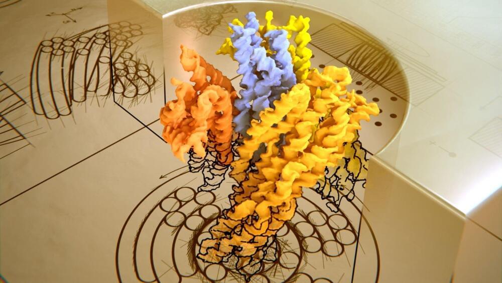
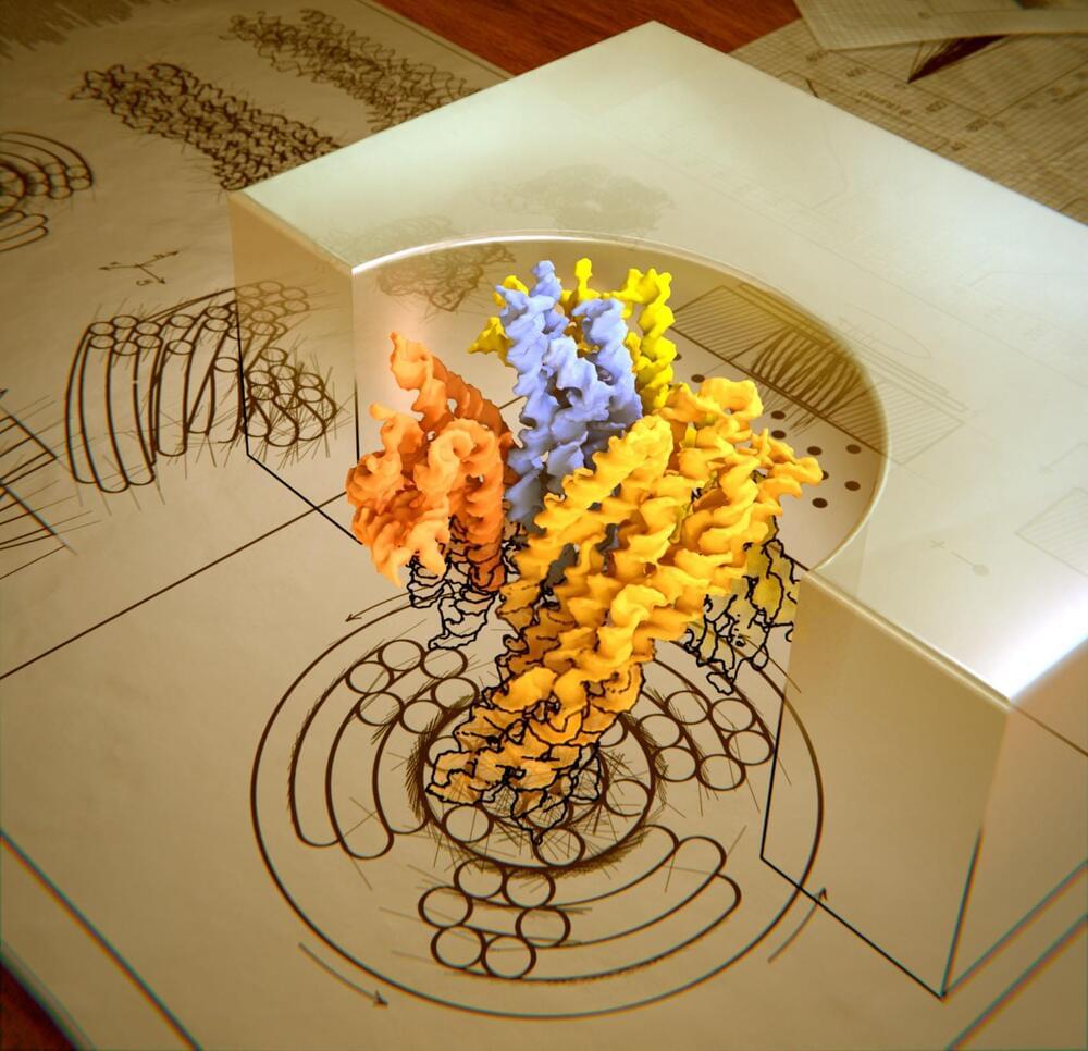
A combination of gentle stimulated emission depletion microscopy imaging and deep-learning-based improvements in signal-to-noise ratio enables high-resolution reconstruction of neuronal architecture in living tissue.
Category: nanotechnology – Page 107
A team of scientists from Sandia National Laboratories and Texas A&M University has recently witnessed for the first time a stunning phenomenon: pieces of metal cracking, then fusing back together without any human intervention.
If this amazing phenomenon can be harnessed, it could give rise to an engineering revolution in which self-healing bridges, engines, or airplanes could reverse damage caused by wear and tear and thus become safer and longer-lasting.
“This was absolutely stunning to watch first-hand,” said Brad Boyce, a materials scientist at Sandia. “What we have confirmed is that metals have their own intrinsic, natural ability to heal themselves, at least in the case of fatigue damage at the nanoscale.”
Over the past decade, teams of engineers, chemists and biologists have analyzed the physical and chemical properties of cicada wings, hoping to unlock the secret of their ability to kill microbes on contact. If this function of nature can be replicated by science, it may lead to development of new products with inherently antibacterial surfaces that are more effective than current chemical treatments.
When researchers at Stony Brook University’s Department of Materials Science and Chemical Engineering developed a simple technique to duplicate the cicada wing’s nanostructure, they were still missing a key piece of information: How do the nanopillars on its surface actually eliminate bacteria? Thankfully, they knew exactly who could help them find the answer: Jan-Michael Carrillo, a researcher with the Center for Nanophase Materials Sciences at the Department of Energy’s Oak Ridge National Laboratory.
For nanoscience researchers who seek computational comparisons and insights for their experiments, Carrillo provides a singular service: large-scale, high-resolution molecular dynamics (MD) simulations on the Summit supercomputer at the Oak Ridge Leadership Computing Facility at ORNL.
Waveguiding scheme enables highly confined subnanometer optical fields.
Researchers have pioneered a novel method for confining light to subnanometer scales. This development offers promising potential for advancements in areas such as light-matter interactions and super-resolution nanoscopy.
Advancements in Light Confinement Technology.
DNA-programmed self-assembly leverages the chemical specificity of DNA hybridization to stabilize user-prescribed crystal structures1,2. Pioneering studies have demonstrated that DNA hybridization can guide the self-assembly of a wide variety of nanoparticle crystal lattices, which can grow to micrometer dimensions and contain millions of particles3,4,5,6,7,8,9. Attention has now turned toward the goal of assembling photonic crystals from optical-scale particles (i.e., roughly 100‑1000 nm in diameter)10,11,12 using DNA-programmed interactions. To this end, progress over the past decade has established that DNA can indeed program the self-assembly of bespoke crystalline structures from micrometer-sized colloidal particles13,14,15,16,17,18,19. However, growing single-domain crystals comprising millions of DNA-functionalized, micrometer-sized colloidal particles remains an unresolved barrier to the development of practical technologies based on DNA-programmed assembly. Prior efforts have yielded either single-domain crystals no more than a few dozen micrometers in size13,14,15,16 or larger polycrystalline materials with heterogeneous domain sizes12,15,17,20. These features—small crystal domains, polycrystallinity, and size dispersity—have therefore precluded the use of DNA-coated colloidal crystals in photonic metamaterial applications.
Assembling macroscopic materials from DNA-functionalized, micrometer-sized colloids is challenging due to the vastly different length scales between the DNA molecules and the colloidal particles (Fig. 1a). This combination leads to crystallization kinetics that are extremely sensitive to temperature and prone to kinetic trapping1,21,22,23. The resulting challenges are both practical and fundamental in nature. For example, recent work has shown that crystal nucleation rates can vary by orders of magnitude over a temperature range of only 0.25 °C19. Extremely precise temperature control would therefore be required to self-assemble single-domain crystals from a bulk solution (Fig. 1b). At the same time, annealing polycrystalline materials is difficult due to the combination of the short-range attraction and the friction arising from the DNA-mediated colloidal interactions, which slows the rolling and sliding of colloidal particles at crystalline interfaces15,19,24,25.
For many, the word “crystals” conjures images of shimmering suncatchers that create a prism of rainbow colors or semi-transparent stones thought to possess healing abilities. But in the realm of science and engineering, crystals take on a more technical definition. They’re perceived as materials whose components – be it atoms, molecules, or nanoparticles –are arranged regularly in space. In other words, crystals are defined by the regular arrangement of their constituents. Familiar examples include diamonds, table salt, and sugar cubes.
Prosthetics moved by thoughts. Targeted treatments for aggressive brain cancer. Soldiers with enhanced vision or bionic ears.
These powerful technologies sound like science fiction, but they’re becoming possible thanks to nanoparticles.
And, as with any great power, there comes great responsibility.
A team at the National Institute of Standards and Technology in Boulder, Colorado, has reported the successful implementation of a 400,000 pixel superconducting nanowire single-photon detector (SNSPD) that they say will pave the way for the development of extremely light-sensitive large-format superconducting cameras. The camera will also prove invaluable for those doing medical research, where the ability to examine organs such as the brain without disturbing tissue is critical.
Superconducting detectors operate at very low temperatures and generate a minimum of excess noise, making them ideal for testing the non-local nature of reality, investigating dark matter, mapping the early universe, and performing quantum computation and communication. Previously there were no large-scale superconducting cameras – even the largest demonstrations have never exceeded 20 thousand pixels.
This was especially true for one of the most promising detector technologies, the superconducting nanowire single-photon detector (SNSPD). These detectors have been demonstrated with system detection efficiencies of 98.0%, sub-3-ps timing jitter, sensitivity from the ultraviolet (250nm) to the mid-infrared (10um), and dark count rates below 6.2e-6 counts per second (cps), but despite more than two decades of development they have never achieved an array size larger than a kilopixel. Here, we report on the implementation and characterization of a 400,000 pixel SNSPD camera, a factor of 400 improvement over the previous state-of-the-art. The array spanned an area 4×2.5 mm with a 5x5um resolution, reached unity quantum efficiency at wavelengths of 370 nm and 635 nm, counted at a rate of 1.1e5 cps, and had a dark count rate of 1e-4 cps per detector (corresponding to 0.13 cps over the whole array).
One of the main ways cells “talk” to each other to coordinate essential biological activities such as muscle contraction, hormone release, neuronal firing, digestion and immune activation is through calcium signaling.
Rice University scientists have used light-activated molecular machines to trigger intercellular calcium wave signals, revealing a powerful new strategy for controlling cellular activity, according to a new study published in Nature Nanotechnology. This technology could lead to improved treatments for people with heart problems, digestive issues and more.
“Most of the drugs developed up to this point use chemical binding forces to drive a specific signaling cascade in the body,” said Jacob Beckham, a chemistry graduate student and lead author on the study. “This is the first demonstration that, instead of chemical force, you can use mechanical force —induced, in this case, by single-molecule nanomachines—to do the same thing, which opens up a whole new chapter in drug design.”
Envision a realm where light can be meticulously controlled and manipulated at minuscule scales, unlocking unprecedented potentials for nanotechnology and quantum information technology. Recent breakthroughs in quantum research have propelled us closer to a reality that may be more achievable than previously realized.
In this article, we delve into the domain of surface plasmon polaritons (SPPs) and the vast possibilities they offer in revolutionizing the field of quantum optics.
Picture a serene lake on a sunny day. As you drop a small stone into the water, it sets in motion gentle ripples that traverse the surface. Now, imagine light as akin to those undulating ripples. When light encounters the interface of a metal and a dielectric material, it has the power to generate waves, much like the ripples on the lake. This phenomenon is even more intriguing because these light waves can interact with the metal’s microscopic constituents, such as electrons. Remarkably, the light waves and electrons synchronize their oscillations, giving rise to an SPP wave.