Those mistakenly identified as under 18 will need to verify their age using a credit card or government-issued ID.

Is Chief Executive Officer and Chairman of the Board of BioStem Technologies (https://biostemtechnologies.com/), a leading innovator focused on harnessing the natural properties of perinatal tissue in the development, manufacture, and commercialization of allografts for regenerative therapies.
Jason brings a wealth of experience in strategic operations planning and technical projects management from his rigorous technical background. His diverse expertise includes continuous process improvement, training and development programs, regulatory compliance and best practices implementation, and advanced problem solving.
Jason began his career as a technical engineer working for Adecco at SC Johnson in 2009, where he developed comprehensive maintenance plans to support manufacturing processes at scale. He then transitioned to manufacturing and quality engineering for major organizations, including ATI Ladish Forging, Nemak, and HUSCO International, where he spearheaded process design and implementation, solved complex supply-chain and manufacturing problems, and improved product sourcing and purchasing.
Jason’s philanthropic work with the Juvenile Diabetes Research Foundation sparked an interest in biotech, leading him to co-found Biostem Technologies in 2014. As CEO he has leveraged his expertise to optimize tissue sourcing, strategically build out a 6,000 square foot tissue processing facility that is fully compliant with FDA 210,211, 1,271, and AATB standards, and put together an expert team of professionals to support the company’s continued growth.
Jason holds a B.S. in Mechanical Engineering Technology and a minor in Mathematics from the Milwaukee School of Engineering and is Six Sigma Black Belt certified. He also serves as a Processing and Distribution Council Member for the American Association of Tissue Banks (AATB), as well as serves as a member of the Government Affairs committee for BioFlorida.
#JasonMatuszewski #BioStemTechnologies #PerinatalTissue #RegenerativeTherapies #ChronicWounds #DiabeticFootUlcers #VenousUlcers #PressureUlcers #AmnioticTissue #TissueAllografts #ExtracellularMatrix #ECM #GrowthFactors #Cytokines #Collagen #ProgressPotentialAndPossibilities #IraPastor #Podcast #Podcaster #ViralPodcast #STEM #Innovation #Technology #Science #Research
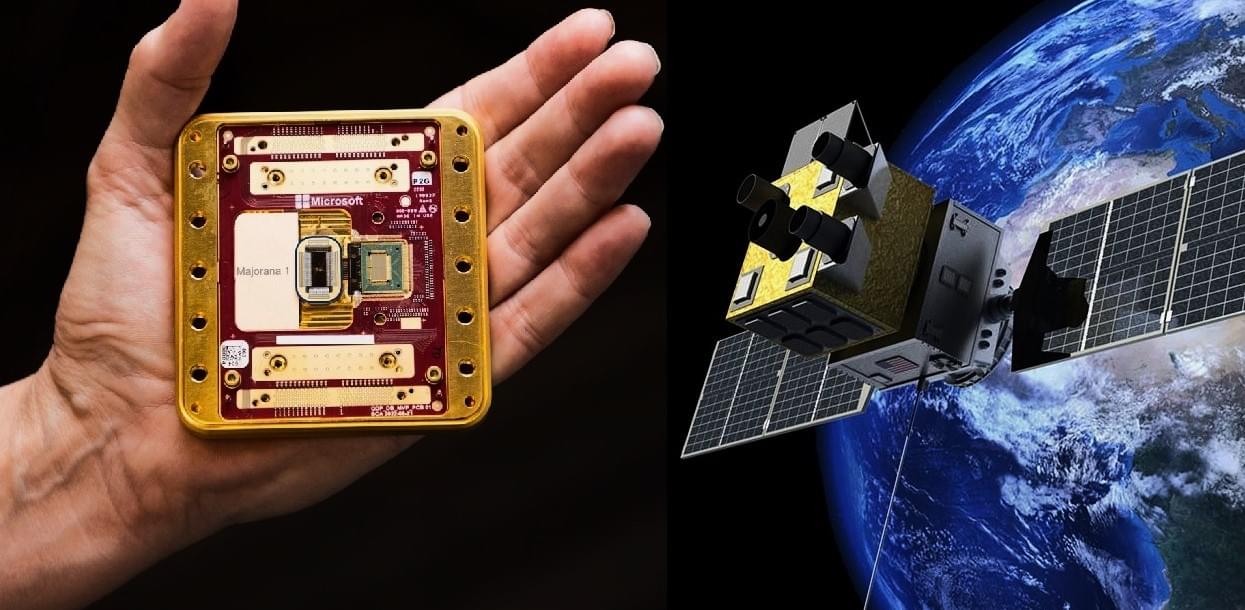
BELLEVUE, Wash. — Quantum physics and outer space may seem as different as two tech frontiers can be, but the challenges facing Pacific Northwest ventures that are aiming to make their fortune on those frontiers are surprisingly similar.
Amid the current turbulence on the national political scene, it’s getting harder to capture the attention — and gain the support — of the federal government, which has historically been the leading funder of research and development. And that means it’s more important than ever for researchers, industry leaders and local officials to join forces.
“Think of it as a triad,” said Jason Yager, executive director of the Montana Photonics and Quantum Alliance, which is one of the beneficiaries of a $41 million Tech Hub grant awarded by the federal government a year ago. “If all of these pieces are working together, then where they meet is socio-economic growth, and then you’re ready to bring in the additional funding to launch that.”
In a world where families are limited to one child due to overpopulation, a set of identical septuplets must avoid being put to a long sleep by the government and dangerous infighting while investigating the disappearance of one of their own.
Our team strives to create quality recaps of your favorite films. On the channel, you will find stories about movies in Sci-Fi, thriller, fantasy, horror, drama, fiction, trash, comedy, detective, psychological thriller, and dystopia genres. Each video will intrigue you with surprises and mystery. Leave the names of your favorite movies in the comments, and we will make an exciting review about each of them.
We will be very grateful if you give us a like for our efforts and subscribe to the channel so as to not miss the next entertaining video. Thank you for watching our recap.
#movierecap #spoilerlab
Last month, Japanese startup foundry Rapidus began prototyping 2-nanometer gate-all-around (GAA) transistors at its new facility, a key step toward ramping up its first production in 2027.
The foundry, which aims to compete with TSMC and Samsung in leading-edge chips for AI, said in a press statement that in about three years, it has reached target milestones, including the fab groundbreaking in September 2023, clean room completion in 2024, and, in June this year, the installation of production equipment.
Rapidus and TSMC are two chipmakers that the Japanese government is relying on to revive the nation’s declining semiconductor industry. Rapidus, if successful, will make leading-edge 2-nm chips for companies like IBM. TSMC is producing 12-to 28-nanometer chips for image sensors and automotive applications at its base in Kumamoto, Japan.


WASHINGTON — The U.S. Space Force estimates it would need more than $4 billion to fund a proliferated low Earth orbit constellation known as MILNET that would provide global communications services, making it the largest item in the service’s fiscal year 2026 “unfunded priorities list” submitted to Congress last week.

Questions to inspire discussion.
🚀 Q: How might Elon Musk’s diverse projects contribute to Tesla’s value? A: Musk’s involvement in AI, energy, transportation, and communication through projects like Tesla, SpaceX, and Neuralink demonstrates his capacity to make progress on multiple fronts, potentially creating significant value for Tesla.
Political Involvement and Economic Strategy.
🏛️ Q: Why is Elon Musk getting involved in politics? A: Musk’s political involvement aims to create a better political system on Earth, addressing the unsustainability of US government spending and debt to avoid a fiscal doom loop.
📊 Q: What is Musk’s strategy to improve the US economy? A: Musk plans to accelerate GDP growth through AI-driven growth, humanoid bots, and reducing government spending and waste, potentially breaking free from the constant 7% growth line of the US stock market.
💰 Q: How could reducing government spending benefit the economy? A: By cutting wasteful spending and implementing a balanced budget requirement, the US could potentially grow its economy faster than its spending, reducing interest costs and freeing up money for other investments.
Rivian CEO RJ Scaringe claims that legacy automakers are intentionally slowing down electric vehicle adoption and hindering competition to protect their profits from gas-powered vehicles, which could threaten their survival and allow newer EV makers like Rivian and Tesla to dominate the market ## ## Questions to inspire discussion.
Legacy Automakers and EVs.
🚗 Q: Why are legacy automakers resistant to selling EVs? A: Legacy automakers don’t want to sell EVs because they make good margins on low-efficiency gas cars and can sell them at a premium price, preferring to see the EV market disappear.
🏛️ Q: How are legacy automakers fighting against EV policies? A: Legacy automakers are the biggest adversaries of EV policies, spending the most energy fighting against them in DC, reflecting their desire for the EV market to vanish. Rivian’s Challenges and Strategy.
💰 Q: What financial challenge does Rivian face? A: Rivian has a massive $23 billion debt, making it more indebted than any startup has ever been, requiring 10–20 years to become cash flow positive.
🛻 Q: How is Rivian addressing its product pricing? A: Rivian’s R2 electric truck, launching in 2025, will target a **$45,000 starting price, a strategic move to make their products more accessible.