Ceramic nanowires could essentially be used even for car tires reducing even hazardous rubber waste.
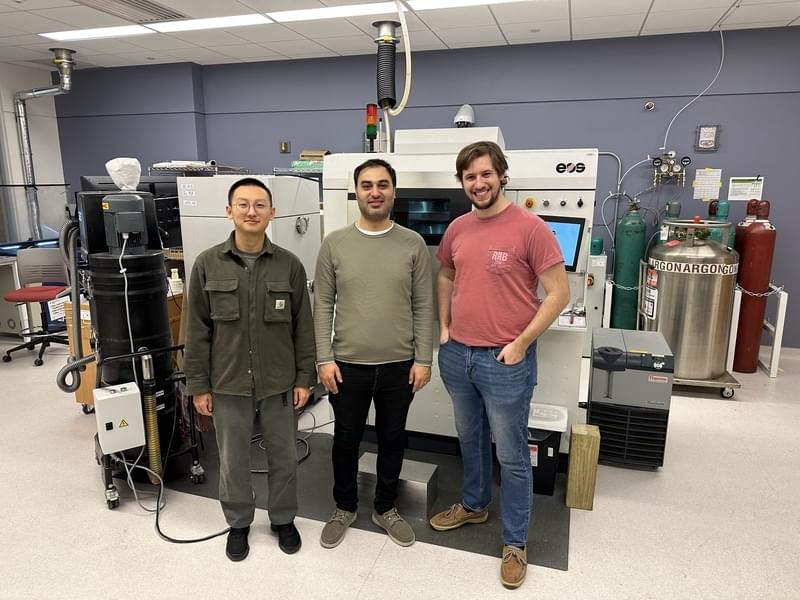
A team of MIT-led engineers found a simple, inexpensive way to strengthen Inconel 718 with ceramic nanowires to be used in metal PBF AM processes. The team believes that their general approach could be used to improve many other materials. “There is always a significant need for the development of more capable materials for extreme environments. We believe that this method has great potential for other materials in the future,” said Ju Li, the Battelle Energy Alliance Professor in Nuclear Engineering and a professor in MIT’s Department of Materials Science and Engineering (DMSE).
Li, who is also affiliated with the Materials Research Laboratory (MRL), is one of three corresponding authors of a paper on the work that appeared in the April 5 issue of Additive Manufacturing. The other corresponding authors are Professor Wen Chen of the University of Massachusetts at Amherst and Professor A. John Hart of the MIT Department of Mechanical Engineering.
Co-first authors of the paper are Emre Tekoğlu, an MIT postdoc in the Department of Nuclear Science and Engineering (NSE); Alexander D. O’Brien, an NSE graduate student; and Jian Liu of UMass Amherst. Additional authors are Baoming Wang, an MIT postdoc in DMSE; Sina Kavak of Istanbul Technical University; Yong Zhang, a research specialist at the MRL; So Yeon Kim, a DMSE graduate student; Shitong Wang, an NSE graduate student; and Duygu Agaogullari of Istanbul Technical University. The study was supported by Eni S.p. A. through the MIT Energy Initiative, the National Science Foundation, and ARPA-E.