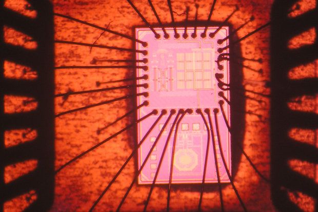
More information on DARPA’s efforts in build new interface standards for modular design & practical circuit blocks.
Is it possible to develop chip technology that combines the high-performance characteristics of ASICS with the speedy, low-cost features of printed circuit boards?
Scientists at the Defense Advanced Research Projects Agency this week said they were looking for information on how to build interface standards that would enable modular design and practical circuit blocks that could be reused to greatly shorten electronics development time and cost.
+More on Network World: DARPA: Researchers develop chip part that could double wireless frequency capacity +
One technique for addressing rising cost and complexity has been the use of a modular design flow that subdivides a system into functional circuit blocks, called IP blocks, DARPA stated. “IP block refers to intellectual property captured in a pre-designed functional circuit block. Examples of IP blocks include, but are not limited to, timing circuits, filters, waveform generators, embedded processors, data converters, amplifiers, fast Fourier transforms, serializer-deserializers and memory,” the agency stated.
