A joint research team has experimentally observed ballistic transport in single-crystalline copper thin films, demonstrating that ballistic transport is achievable in an industry-standard metal at interconnect-relevant dimensions. The study, titled “Ballistic transport in nanodevices based on single-crystalline Cu thin films,” was published in Nature Communications.
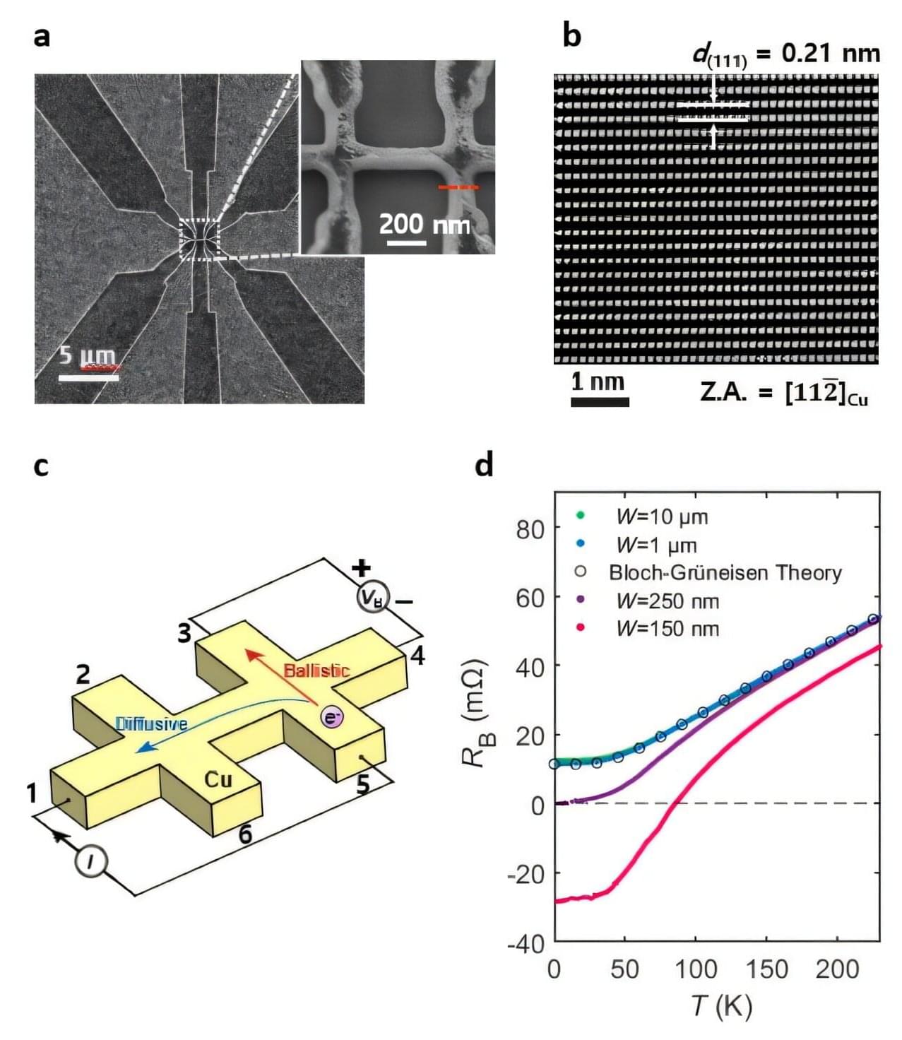
Ballistic transport refers to a phenomenon in which electrons travel along straight trajectories without scattering. Until now, this behavior has mainly been observed in special quantum materials such as graphene or semiconductor nanostructures. In copper, where electron scattering is pronounced, realizing ballistic transport has been considered practically impossible.
In this study, the team led by Professor Gil-Ho Lee of the Department of Physics at POSTECH, Professor Emeritus Se-Young Jeong of the School of Transdisciplinary Engineering at Pusan National University and Professor Seong-Gon Kim of the Department of Physics and Astronomy at Mississippi State University, experimentally demonstrated that ballistic transport can occur in structures with a thickness of 80 nm and a linewidth of 150 nm, dimensions comparable to those used in semiconductor interconnects.