Perovskites are a class of materials with a unique crystal structure that suits applications such as fabricating solar cells, light-emitting diodes and transistors. However, molecules in thin layers often cannot arrange themselves properly because the process proceeds too quickly. Now, an international research team led by Tomasz Marszalek from the Max Planck Institute for Polymer Research has developed a new approach to controlling low-cost solution processing, thereby improving the formation of well-ordered perovskite layers and enabling their broader application in optoelectronic devices. Their paper is published in the Journal of the American Chemical Society.
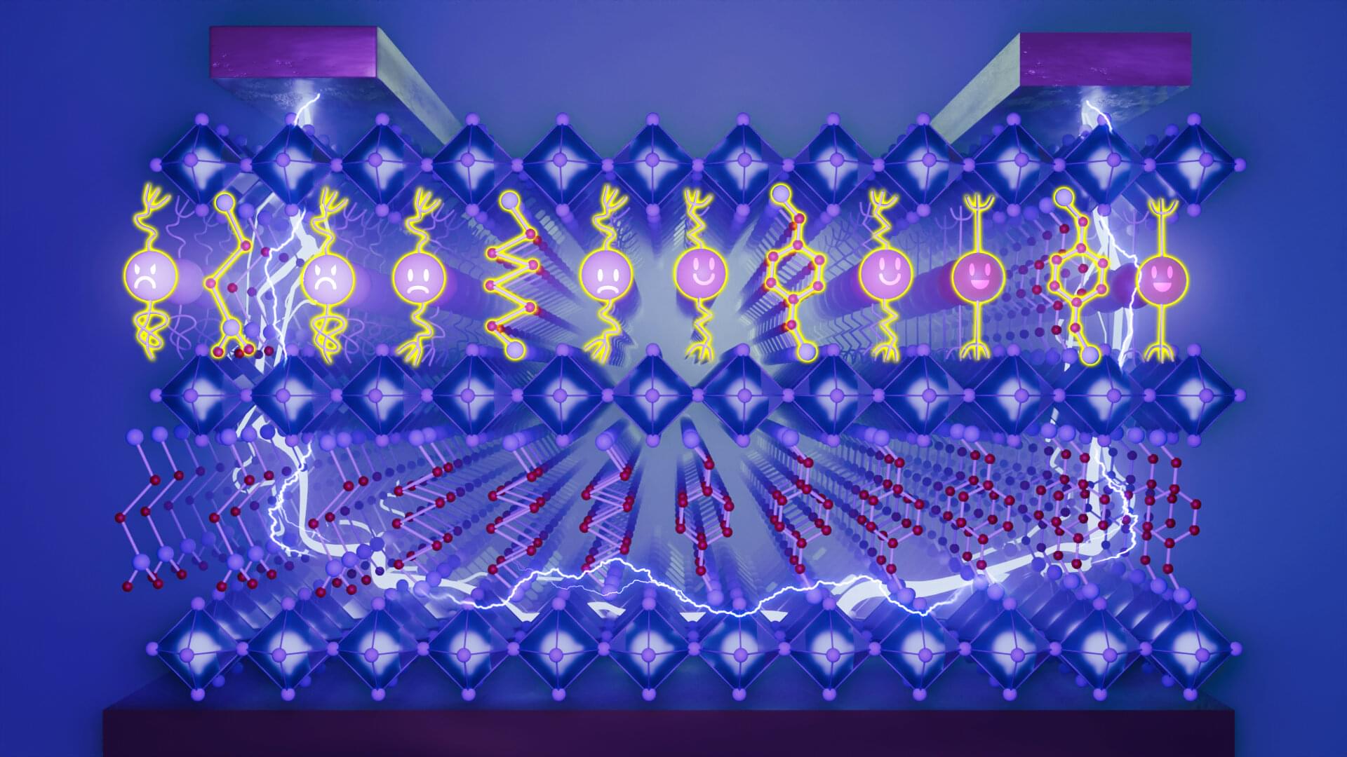
Electronics can be found in almost every device, from smartphones and televisions to washing machines. Field-effect transistors are the main building blocks of electronic circuits, and they ensure that these devices can be easily operated and fully controlled. Perovskites are a new class of semiconductor that could be suitable for transistor applications. They contain various chemical elements, such as organic cations, divalent metal cations, and halide anions. This combination of elements enables the properties of thin perovskite films to be tailored precisely for specific applications.
Currently, their use in transistors is often unsuccessful due to a lack of control over the formation of the thin film, known as nucleation and crystallization. Therefore, researchers are attempting to organize the materials into thin, two-dimensional layers and stabilize them with organic molecules between the inorganic layers in order to control their optoelectronic properties.