Two-dimensional (2D) semiconducting materials have distinct optoelectronic properties that could be advantageous for the development of ultra-thin and tunable electronic components. Despite their potential advantages over bulk semiconductors, optimally interfacing these materials with gate dielectrics has so far proved challenging, often resulting in interfacial traps that rapidly degrade the performance of transistors.
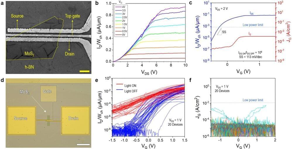
Researchers at King Abdullah University of Science and Technology (KAUST), Soochow University and other institutes worldwide recently introduced an approach that could enable the fabrication of better performing transistors based on 2D semiconductors. Their proposed design, outlined in a paper in Nature Electronics, entails the use of hexagonal boron nitride (h-BN) dielectrics and metal gate electrodes with a high cohesive energy.
“Initially, we found that when we use platinum (Pt) as an anode, the h-BN stack is less likely to trigger dielectric breakdown,” Yaqing Shen, first author of the paper, told Tech Xplore. “Based on this finding, we designed our experiments and found that Pt/h-BN gate stacks show 500-times lower leakage current than Au/h-BN gate stacks and exhibit a high dielectric strength of at least 25 MV/cm. This gave us the idea of using CVD h-BN as a gate dielectric in 2D transistors.”