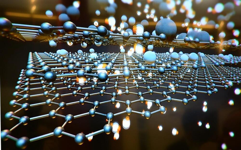
Two-dimensional materials, which are only a few atoms thick, can exhibit some incredible properties, such as the ability to carry electric charge extremely efficiently, which could boost the performance of next-generation electronic devices.
However, integrating 2D materials into devices and systems like computer chips is notoriously difficult. These ultrathin structures can be damaged by conventional fabrication techniques, which often rely on the use of chemicals, high temperatures, or destructive processes like etching.
To overcome this challenge, researchers from MIT and elsewhere have developed a new technique to integrate 2D materials into devices in a single step while keeping the surfaces of the materials and the resulting interfaces pristine and free from defects.
