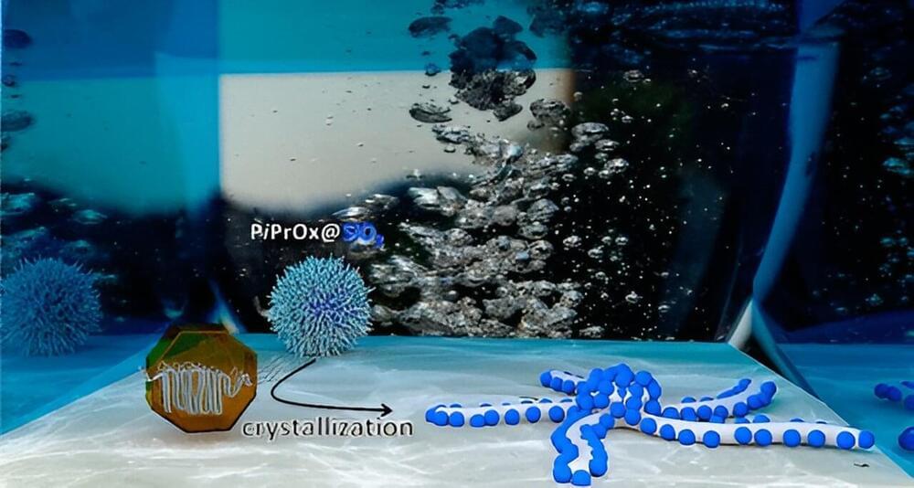
Scientists from the Friedrich Schiller University Jena and the Friedrich Alexander University Erlangen-Nuremberg, both Germany, have successfully developed nanomaterials using a so-called bottom-up approach. As reported in the journal ACS Nano, they exploit the fact that crystals often grow in a specific direction during crystallization. These resulting nanostructures could be used in various technological applications.
“Our structures could be described as worm-like rods with decorations,” explains Prof. Felix Schacher. “Embedded in these rods are spherical nanoparticles; in our case, this was silica. However, instead of silica, conductive nanoparticles or semiconductors could also be used—or even mixtures, which can be selectively distributed in the nanocrystals using our method,” he adds. Accordingly, the range of possible applications in science and technology is broad, spanning from information processing to catalysis.
“The primary focus of this work was to understand the preparation method as such,” explains the chemist. To produce nanostructures, he elaborates, there are two different approaches: larger particles are ground down to nanometer size, or the structures are built up from smaller components.
