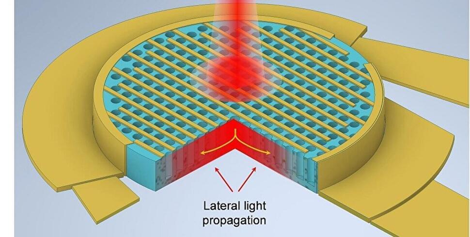
Photonic systems are quickly gaining traction in many emerging applications, including optical communications, lidar sensing, and medical imaging. However, the widespread adoption of photonics in future engineering solutions hinges on the cost of manufacturing photodetectors, which, in turn, largely depends on the kind of semiconductor utilized for the purpose.
Traditionally, silicon (Si) has been the most prevalent semiconductor in the electronics industry, so much so that most of the industry has matured around this material. Unfortunately, Si has a relatively weak light absorption coefficient in the near-infrared (NIR) spectrum compared to those of other semiconductors such as gallium arsenide (GaAs).
Because of this, GaAs and related alloys thrive in photonic applications, but are incompatible with the traditional complementary metal-oxide-semiconductor (CMOS) processes used in the production of most electronics. This leads to a drastic increase in their manufacturing costs.
