T cells are a powerful weapon in the fight against cancer, forming the basis of treatments such as CAR-T cell therapy and checkpoint inhibitors. This research centers on another type of immunotherapy approach called T cell receptor (TCR) therapy, which engineers T cells to recognize specific proteins on cancer cells, allowing for highly targeted attacks.
Many of these proteins, however, are “self-antigens,” or molecules normally found in the body. To prevent these T cells from attacking healthy tissue, the immune system naturally eliminates the strongest cancer-fighting T cells during development. This leaves behind weaker T cell receptors that may struggle to recognize and destroy tumors, particularly those that have learned to evade immune defenses.
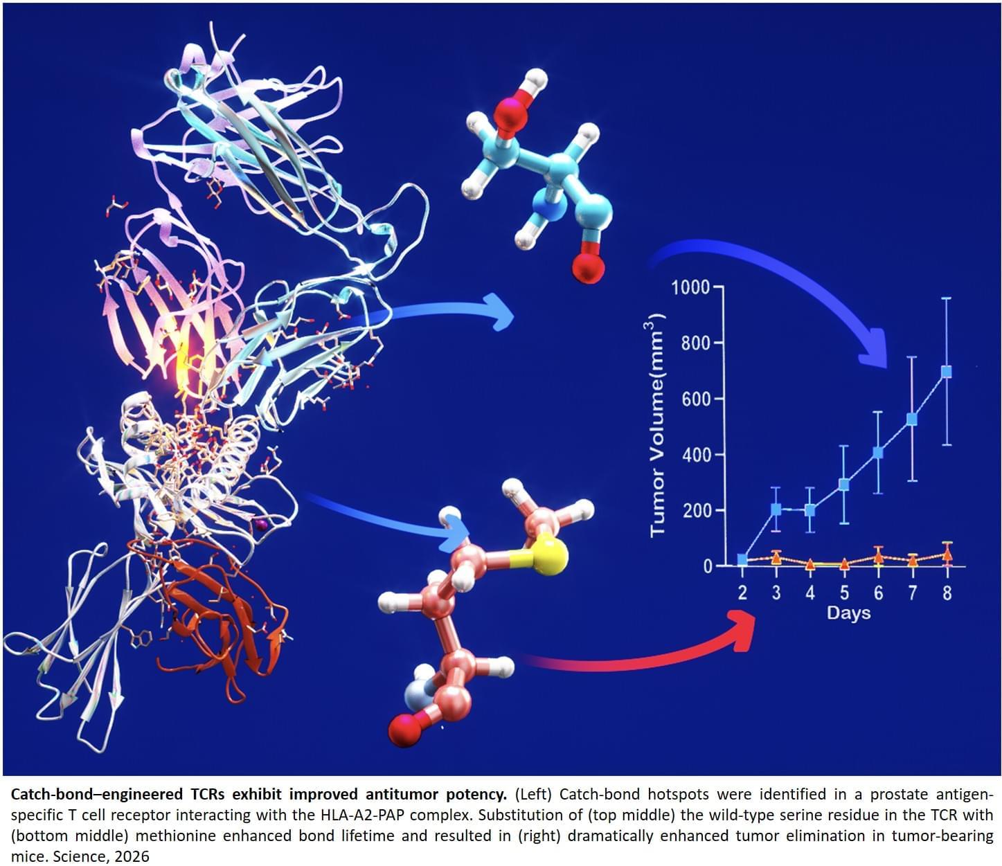
To overcome this challenge, researchers focused on fine-tuning naturally occurring T cell receptors to strengthen their ability to recognize a common prostate cancer protein called prostatic acid phosphatase (PAP), which is commonly expressed on prostate tissue and prostate tumors. The team identified a naturally weak TCR, known as TCR156, that could detect PAP but was not strong enough to effectively kill cancer cells.
Using a novel technique called catch bond engineering, a concept developed by the Lab, the researchers “turbocharged” the T cells. In the body, T cells form brief, mechanical bonds with their targets, known as catch bonds, which help them sense and respond to threats. By altering just one or two amino acids in the T cell receptor, the scientists were able to strengthen these bonds while preserving the T cells’ natural ability to recognize their specific target.
Multiple engineered versions of TCR156 were created and tested. Two candidates proved to be the most effective. These engineered T cells were analyzed for their ability to recognize tumors, release cancer-killing molecules, proliferate, and resist exhaustion. Advanced imaging, single-cell RNA sequencing, and structural analyses were used to confirm that the modifications improved T cell function while maintaining precision and avoiding off-target effects.
Structural and computer modeling studies showed that the catch bond mutations did not change the overall TCR shape but primed it to form a new interaction with PAP when the T cell engaged the tumor, explaining how the engineered T cells could remain highly specific while dramatically boosting their cancer-killing ability.
The researchers found that a single amino acid change created a catch bond hotspot that significantly enhanced T cell function. This change did not directly contact the cancer protein until the T cell engaged dynamically, demonstrating that a tiny modification can have a major effect. Most importantly, the modifications did not make the cells attack healthy tissue.