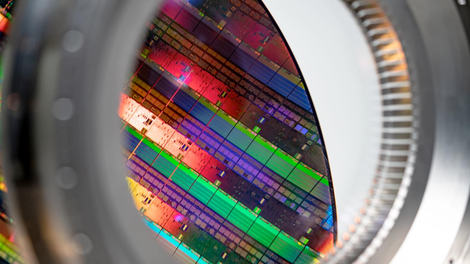
Lace Lithography, a Norwegian start-up backed by Microsoft, raised $40 million in Series A funding on Monday to develop a chipmaking tool that uses a helium atom beam instead of light to pattern silicon wafers, Reuters reported. The company claims its technology can create chip features 10 times smaller than current lithography systems, with a beam width of just 0.1 nanometers compared to the 13.5nm wavelength used by ASML’s EUV scanners. Lace aims to have a test tool running in a pilot fab by 2029.
The advantage of Lace’s system is that atoms don’t have a diffraction limit, whereas photon-based lithography, including ASML’s EUV systems, is constrained by the wavelength of the light it uses. As chipmakers push features smaller, they rely on increasingly complex multi-patterning techniques to work around that limit, but Lace sidesteps the problem entirely by replacing photons with neutral helium atoms and a beam measuring roughly the width of a single hydrogen atom.

