Atomically thin semiconductors such as tungsten disulfide (WS2) are promising materials for future photonic technologies. Despite being only a single layer of atoms thick, they host tightly bound excitons—pairs of electrons and holes that interact strongly with light—and can efficiently generate new colors of light through nonlinear optical processes such as second-harmonic generation.
These properties make them attractive for quantum optics, sensing, and on-chip light sources. At the same time, their extreme thinness imposes a basic limitation: There is very little material for light to interact with. As a result, emission and frequency conversion are often weak unless the surrounding photonic environment is carefully engineered.
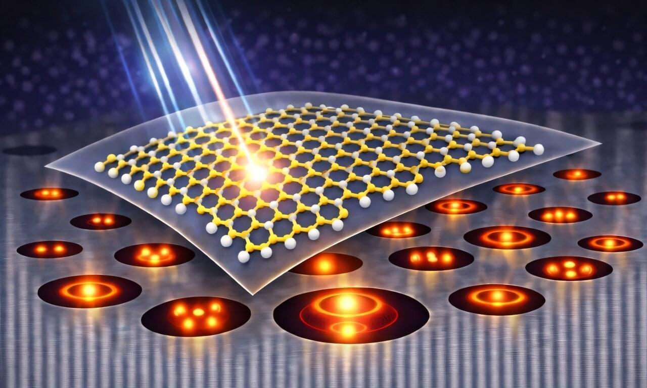
A study published in Advanced Photonics introduces a new way to address this challenge by reshaping not the two-dimensional material itself, but the space beneath it. The researchers demonstrate a hybrid platform in which a monolayer of WS2 is placed on top of nanoscale air cavities, known as Mie voids, carved into a high-index crystal of bismuth telluride (Bi2Te3). The work shows that these voids can strongly enhance light emission and nonlinear optical signals, while also allowing direct visualization of localized optical modes.