Toggle light / dark theme

The Future Will Be Shaped By Accelerated Technological Development And Visionary Leadership

Chuck Brooks is the president of Brooks Consulting International and one of Executive Mosaic’s GovCon Experts.

We are on the brink of a transformative era where rising technologies are colliding to create unparalleled innovation. artificial intelligence, nanotechnology and quantum technologies are transforming research and development, expediting prototyping and disrupting various industries.

This convergence, propelled by exponential processing power, molecular precision and intelligent systems, promises trillions in economic value while posing significant concerns in security, ethics and labor preparedness.

New method brings single-particle quality control to nanocrystal manufacturing

Nanocrystals are already used in millions of devices, including televisions, laptops and displays, and are considered key materials for the next generation of quantum, sensing and solar technologies. However, they have not yet fully realized their potential. One major reason is their inherent heterogeneity: A single solution contains billions of nanocrystals whose properties can differ substantially. Although these particles can be characterized, important quality parameters are typically accessible only as average values across the entire sample.

“For their function in devices, these average values are insufficient,” says Professor Emiliano Cortés, who conducts research at LMU’s Nano-Institute. “Each individual nanoparticle can behave differently—for example, in its size or in how efficiently it emits light, meaning how effectively it converts absorbed energy back into light.”

China supercharges AI with 100-fold faster optical chip breakthrough

A PERSONAL SUPER COMPUTER “MACRO-CHIP” WITH PHOTONIC INTERCONNECTS:

This will soon become possible by the cheap nano-imprinting of hundreds of smaller microchips, without the need for laser lithography, onto a single monolithic wafer, with these chips’ communicating with each other at light speed as a single system via silicon photonics. A team at Peking University has set this race in motion in a major way by developing an optical system to boost AI speeds 100-fold by optical interconnects between individual microchips. The next step will be placing all of those chips onto a single monolithic wafer with a similar communication system between them. Nano-imprinting at large node-scale of 15 or 20 nm will make it possible to mass produce wafer scale systems that combine all the best types of computing features, from logic gates to optical AI accelerators in one compact package on a single wafer. Consumers will not care if the computer chips in their computers are not 14-mm wide 2-nm node chips printed by expensive extreme ultraviolet lithography, but are, instead, 8-inch or 12-inch wide super computer “macro-chips” that give 1,000 times the computing power and speed of the best Nvidia computer on the market today, whereon the distance of the individual chiplets on the wafer from the central optical multiplexer becomes part of the ingrained clock feature of the chip, replacing the traditional clock-time limit. The mother boards, GPUs and CPUs of these systems will all exist on the same wafer and communicate at light speed, with the equivalent of something like 1,000 VRAM of unified memory.

These developments come as the shrinking of traditional silicon microchips is facing a final limit. In the same way that the Personal Computer became the game-changer in the 1980’s, it appears that Personal Super-Computers will become the new kid on the block in the 2030’s.


Peking University researchers develop new all-optical interconnect system linking standard electronic chips with specific algorithms.

Researchers find simple solution for extending the lifespan of LEDs made from glowing quantum dots

A new study led by MIT researchers could drive the development of more energy-efficient digital displays—such as flat-screen TVs, augmented and virtual reality headsets, smartphone screens, medical imaging devices and even large-area ambient lighting surfaces—that also generate richer, brighter colors.

The MIT scientists, in collaboration with researchers at Samsung, studied the microscopic changes that occur inside LEDs that use electrically excited quantum dots, which are precisely shaped nanoscale semiconductor particles that emit extremely pure colored light. The research appears in Science Advances.

Quantum dots are currently used in some of the computer and television displays with the best picture quality available. The efficiency of these displays could be further improved, and their manufacturing process further simplified, if the quantum dots could be electrically excited, as was first demonstrated in the quantum dot LED (QD-LED) structures more than 20 years ago.

Common nanostructures may explain shared photoproperties in two widespread dark materials

A newly developed framework for understanding the photoproperties of both natural organic matter and eumelanin, a natural pigment responsible for dark colors in organisms, may inspire advanced sustainable technologies, scientists say.

Although they are some of the most widespread substances on Earth, not much is known about eumelanin or natural organic matter (NOM)—a dark-colored substance formed by the decomposition of biological material. In humans, eumelanin is a vital pigment in skin and other tissues that protects cells from damage caused by ultraviolet radiation. In nature, NOM gives rivers and soils their color and affects light-driven reactions like photosynthesis.

Although these compounds have been studied individually for decades, researchers in a new study, by scrutinizing them alongside each other, have shown that eumelanin and NOM have common properties beyond their dark colors.

New optical centrifuge unlocks the secrets of frictionless superfluids

Physicists have developed a new way to control the rotation of molecules inside tiny droplets of liquid helium, marking an important advance in the study of superfluids. By using a specially designed optical centrifuge, the team was able to precisely spin molecules suspended in liquid helium nano-droplets, giving scientists a powerful new tool for exploring these unusual frictionless materials.

The achievement represents the first successful demonstration of controlled molecular rotation inside a superfluid. Researchers can now directly adjust both the direction and speed of a molecule’s rotation, making it possible to investigate how molecules interact with their quantum surroundings at different rotational frequencies. The work, led by researchers at the University of British Columbia (UBC) in collaboration with the University of Freiburg, was published in Physical Review Letters.

“Controlling the rotation of a molecule dissolved in any fluid is a challenge,” said Dr. Valery Milner, associate professor with UBC Physics and Astronomy and author on the paper.

Nanozymes map nanoparticle routes inside live cells without genetic engineering

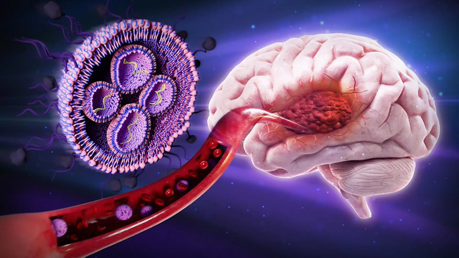
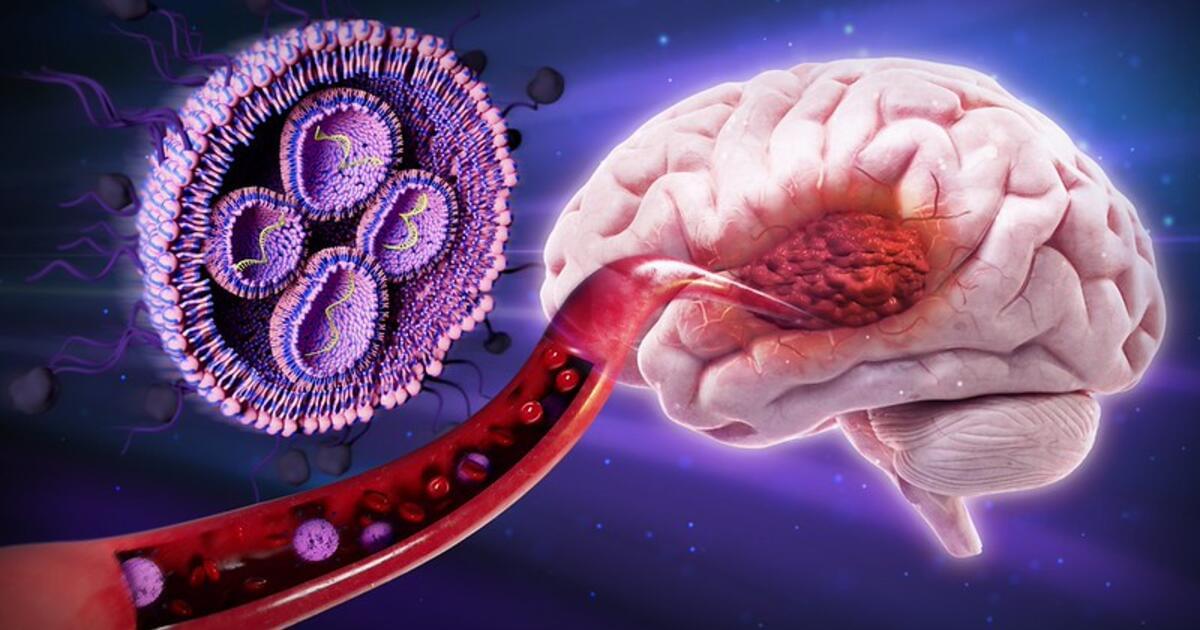
Nanoparticles are widely used in medicine to deliver drugs, genes or imaging agents to specific parts of the body. Once a nanoparticle reaches a cell, however, many things can happen—it can reach its target, be degraded, interact with proteins that help transport it, or interact with proteins that hinder its transport.

A longstanding problem in designing nanomedicines has been understanding what happens to nanoparticles at the cellular level, but scientists have faced many challenges. For example, optical microscopy imaging techniques provide only a generalized view of nanomedicine localization.

On the other hand, proteomics approaches require cell lysis, which disrupts the natural distribution of proteins around the nanoparticle, making it difficult to understand how nanoparticles are transported within the cell. Another method—proximity labeling—enables in situ investigation of intracellular protein-protein interactions, but it relies on genetically engineered enzyme fusion, which limits its applicability across diverse systems.

/* */