Electrons in a magnetic field can display striking behaviors, from the formation of discrete energy levels to the quantum Hall effect. These discoveries have shaped our understanding of quantum materials and topological phases of matter. Light, however, is made of neutral particles and does not naturally respond to magnetic fields in the same way. This has limited the ability of researchers to reproduce such effects in optical systems, particularly at the high frequencies used in modern communications.
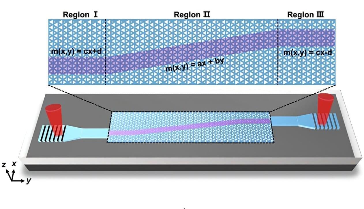
To address this challenge, researchers from Shanghai Jiao Tong University and Sun Yat-Sen University have developed a method for generating pseudomagnetic fields—synthetic fields that mimic the influence of real magnetic fields—inside nanostructured materials known as photonic crystals.
Unlike previous demonstrations, which focused on specific effects such as photonic Landau levels, the new approach allows arbitrary control of how light flows within the material. Their research is published in Advanced Photonics.