Menu

Blog

Archive for the ‘nanotechnology’ category: Page 39

Jun 7, 2023

Revolutionary 3D Printing Technology a “Game Changer” for Discovering and Manufacturing New Materials

Posted by in categories: 3D printing, computing, nanotechnology, solar power, sustainability

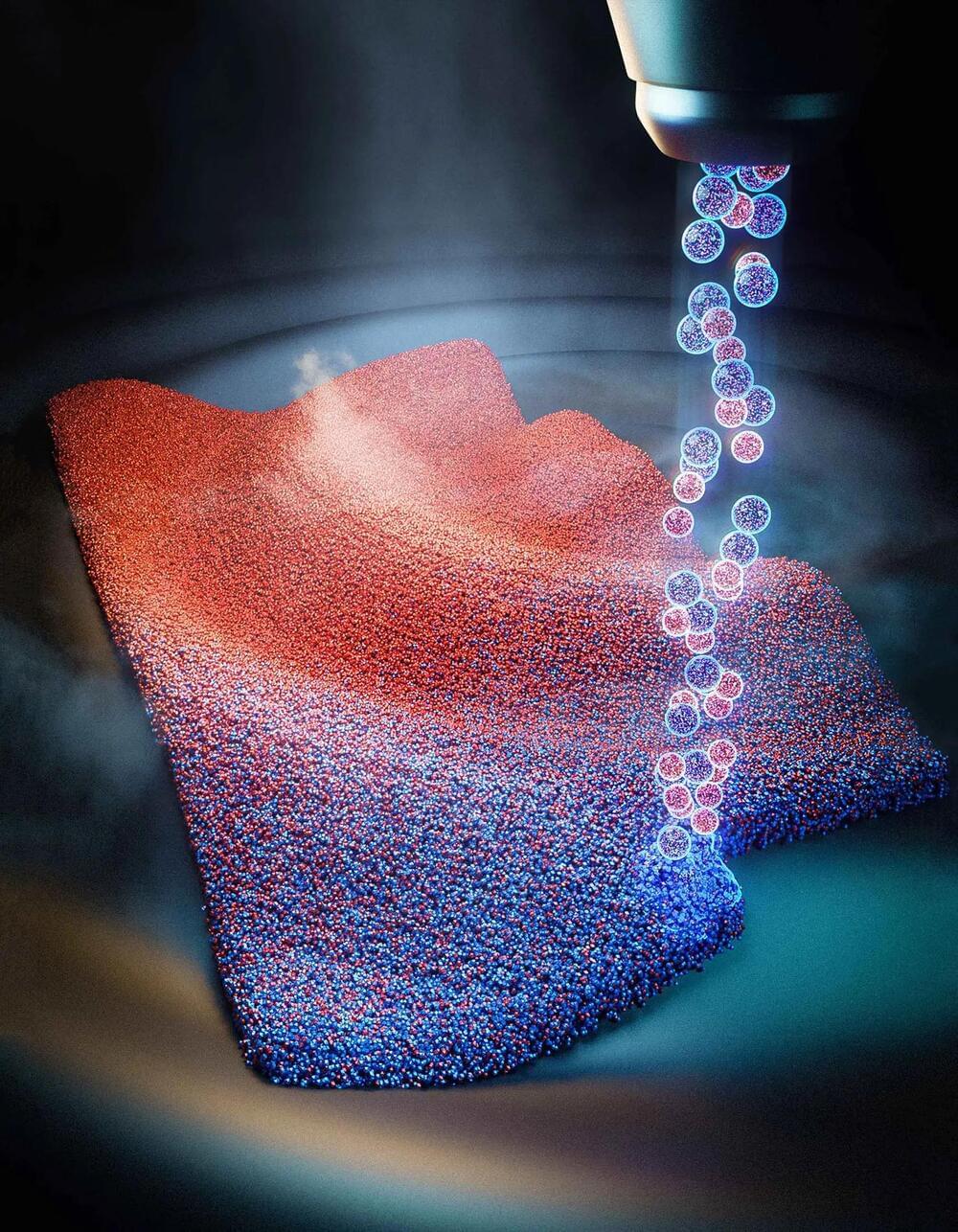
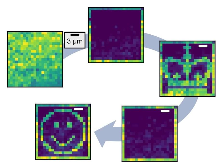
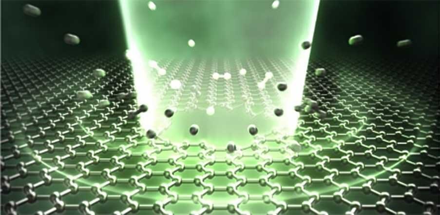
A novel 3D printing method called high-throughput combinatorial printing (HTCP) has been created that significantly accelerates the discovery and production of new materials.

The process involves mixing multiple aerosolized nanomaterial inks during printing, which allows for fine control over the printed materials’ architecture and local compositions. This method produces materials with gradient compositions and properties and can be applied to a wide range of substances including metals, semiconductors.

Semiconductors are a type of material that has electrical conductivity between that of a conductor (such as copper) and an insulator (such as rubber). Semiconductors are used in a wide range of electronic devices, including transistors, diodes, solar cells, and integrated circuits. The electrical conductivity of a semiconductor can be controlled by adding impurities to the material through a process called doping. Silicon is the most widely used material for semiconductor devices, but other materials such as gallium arsenide and indium phosphide are also used in certain applications.

Jun 5, 2023

Creating complex protocells and prototissues using simple DNA building blocks Communications

Posted by in categories: bioengineering, biotech/medical, nanotechnology

Legitimately awesome paper wherein Arulkumaran et al. assemble DNA nanotubes and use them to build artificial ‘cytoskeletons’ inside of giant unilamellar vesicles. They go on to make a variety of fun variations on this theme and eventually build artificial ‘tissues’ made up of these synthetic cell-like vesicles and an ‘extracellular matrix’ that is also made of DNA nanotubes. I find this paper impressive due to how performs precise engineering at the nanoscale and builds up layers of complexity until macroscale specimens are created in a fashion reminiscent of biological systems, yet unique in its own way. #biotechnology #nanotechnology #cellbiology #bioengineering


Building synthetic protocells and prototissues hinges on the formation of biomimetic skeletal frameworks. Here, the authors harness simplicity to create complexity by assembling DNA subunits into structural frameworks which support membrane-based protocells and prototissues.

Jun 5, 2023

This Week’s Awesome Tech Stories From Around the Web (Through June 3)

Posted by in categories: internet, nanotechnology, robotics/AI

From the surreal world of AI-generated films to a nanoscale robotic hand, check out this week’s awesome tech stories from around the web.

Jun 4, 2023

Understanding the tantalizing benefits of tantalum for improved quantum processors

Posted by in categories: chemistry, computing, nanotechnology, quantum physics

Whether it’s baking a cake, building a house, or developing a quantum device, the quality of the end product significantly depends on its ingredients or base materials. Researchers working to improve the performance of superconducting qubits, the foundation of quantum computers, have been experimenting using different base materials in an effort to increase the coherent lifetimes of qubits.

The coherence time is a measure of how long a retains quantum information, and thus a primary measure of performance. Recently, scientists discovered that using tantalum in makes them perform better, but no one has been able to determine why—until now.

Scientists from the Center for Functional Nanomaterials (CFN), the National Synchrotron Light Source II (NSLS-II), the Co-design Center for Quantum Advantage (C2QA), and Princeton University investigated the fundamental reasons that these qubits perform better by decoding the chemical profile of tantalum.

Jun 3, 2023

Buckle up: A new class of materials is here

Posted by in categories: engineering, nanotechnology

Usually, the two characterizations of a material are mutually exclusive: something is either stiff, or it can absorb vibrations well—but rarely both. However, if we could make materials that are both stiff and good at absorbing vibrations, there would be a whole host of potential applications, from design at the nanoscale to aerospace engineering.

A team of researchers from the University of Amsterdam has now found a way to create that are stiff, but still good at absorbing vibrations—and equally importantly, that can be kept very light-weight.

Continue reading “Buckle up: A new class of materials is here” »

Jun 1, 2023

A new approach to realize parallel in-memory wireless computing

Posted by in categories: computing, internet, nanotechnology

Advanced communication technologies, such as the fifth generation (5G) mobile network and the internet of things (IoT) can greatly benefit from devices that can support wireless communications while consuming a minimum amount of power. As most existing devices have separate components to perform computations and transmit data, reducing their energy consumption can be challenging.

Researchers at Nanjing University, Southeast University and Purple Mountain Laboratories in China recently devised a parallel in-memory wireless computing scheme that performs computations and concurrently on the same hardware. This design, introduced in Nature Electronics, is based on the use of mermristive crossbar arrays, grid-like structures containing memristors, electrical components that can both process and store data.

“In one of our previous works published in Nature Nanotechnology, we proposed the realization of massively parallel in-memory computing by using continuous-time data representation in a nanoscale crossbar array,” Shi-Jun Liang, one of the researchers who carried out the recent study, told Tech Xplore.

May 31, 2023

Examining a nanocrystal that shines on and off indefinitely

Posted by in categories: engineering, nanotechnology

In 2021, lanthanide-doped nanoparticles made waves—or rather, an avalanche—when Changwan Lee, then a Ph.D. student in Jim Schuck’s lab at Columbia Engineering, set off an extreme light-producing chain reaction from ultrasmall crystals developed at the Molecular Foundry at Berkeley Lab. Those same crystals are back again with a blink that can now be deliberately and indefinitely controlled.

“We’ve found the first fully photostable, fully photoswitchable nanoparticle—a holy grail of nanoprobe design,” said Schuck, associate professor of mechanical engineering.

This unique material was synthesized in the laboratories of Emory Chan and Bruce Cohen at the Molecular Foundry, Lawrence Berkeley National Laboratory as well as in a national lab in South Korea. The research team also included Yung Doug Suh’s lab at Ulsan National Institute of Science and Technology (UNIST).

May 30, 2023

The Woman Who Doesn’t Feel Pain — New Study Reveals Her Unique Molecular Machinery

Posted by in categories: biotech/medical, genetics, nanotechnology

New research from UCL, investigating the biology of a rare genetic mutation that enables carrier Jo Cameron to live virtually without pain and fear while also healing quickly, discovered that the mutation in FAAH-OUT gene ‘turns down’ FAAH gene expression, affecting molecular pathways related to wound healing and mood, thereby offering potential new targets for drug discovery.

New research from University College London (UCL) has unraveled the biology behind a unique genetic mutation that results in its carrier experiencing minimal pain, enhanced healing, and lower levels of anxiety and fear.

Published in the journal Brain, the research is a follow-up to the team’s 2019 discovery of the FAAH-OUT gene and its rare mutations, which make Jo Cameron almost immune to pain, and devoid of fear and anxiety. The latest study elucidates how this mutation reduces the expression of the FAAH gene and impacts other molecular pathways associated with mood and wound healing. The insights garnered from these findings could potentially pave the way for novel drug targets and foster further research in these domains.

May 28, 2023

Team successfully demonstrates laser-induced monolayer graphene nanoprocessing

Posted by in categories: computing, nanotechnology

Discovered in 2004, graphene has revolutionized various scientific fields. It possesses remarkable properties like high electron mobility, mechanical strength, and thermal conductivity. Extensive time and effort has been invested in exploring its potential as a next-generation semiconductor material, leading to the development of graphene-based transistors, transparent electrodes, and sensors.

But to render these devices into practical application, it’s crucial to have efficient processing techniques that can structure films at micrometer and nanometer scale. Typically, micro/nanoscale material processing and device manufacturing employ nanolithography and focused ion beam methods. However, these have posed longstanding challenges for laboratory researchers due to their need for large-scale equipment, lengthy manufacturing times, and complex operations.

In January 2023, Tohoku University researchers created a technique that could micro/nanofabricate silicon nitride devices with thicknesses ranging from five to 50 nanometers. The method employed a femtosecond laser, which emitted extremely short, rapid pulses of light. It turned out to be capable of quickly and conveniently processing thin materials without a vacuum environment.

May 28, 2023

Advances in Nanoelectrochemistry: Enabling New Discoveries in Small Volume Chemistry

Posted by in categories: chemistry, education, nanotechnology

In this interview conducted at Pittcon 2023 in Philadelphia, Pennsylvania, we spoke to Dr. Jeffrey Dick about his work studying the chemistry of small volumes and nano-electrochemical tools.

What is your background, and what first attracted you to this field?

My name is Jeffrey Dick, and I grew up in Muncie, Indiana. I studied chemistry at Ball State University and fell in love with research and education.

Page 39 of 264First3637383940414243Last