Two-dimensional (2D) semiconducting materials have proved to be very promising for the development of various electronic devices, including wearables and smaller electronics. These materials can have significant advantages over their bulky counterparts, for instance retaining their carrier mobility irrespective of their reduced thickness.
Despite their promise for creating thin electronics, 2D semiconductors have so far only rarely been used to create monolayer transistors, thinner versions of the crucial electronic components used to modulate and amplify electrical current inside most existing devices. Most proposed monolayer transistors based on 2D semiconductors were created using a few carefully selected materials known to have relatively stable lattice structures, such as graphene, tungsten diselenide or molybdenum disulfide (MoS2).
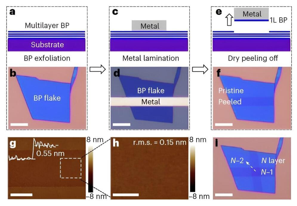
Researchers at Hunan University, the Chinese Academy of Sciences and Wuhan University recently set out to develop new monolayer transistors using alternative 2D semiconducting materials that have so far been primarily used to create multi-layer transistors, including black phosphorus (BP) and germanium arsenide (GeAs). Their work is published in the journal Nature Electronics.