Toggle light / dark theme

Three-in-one diode integrates sensing, memory and processing for smart cameras

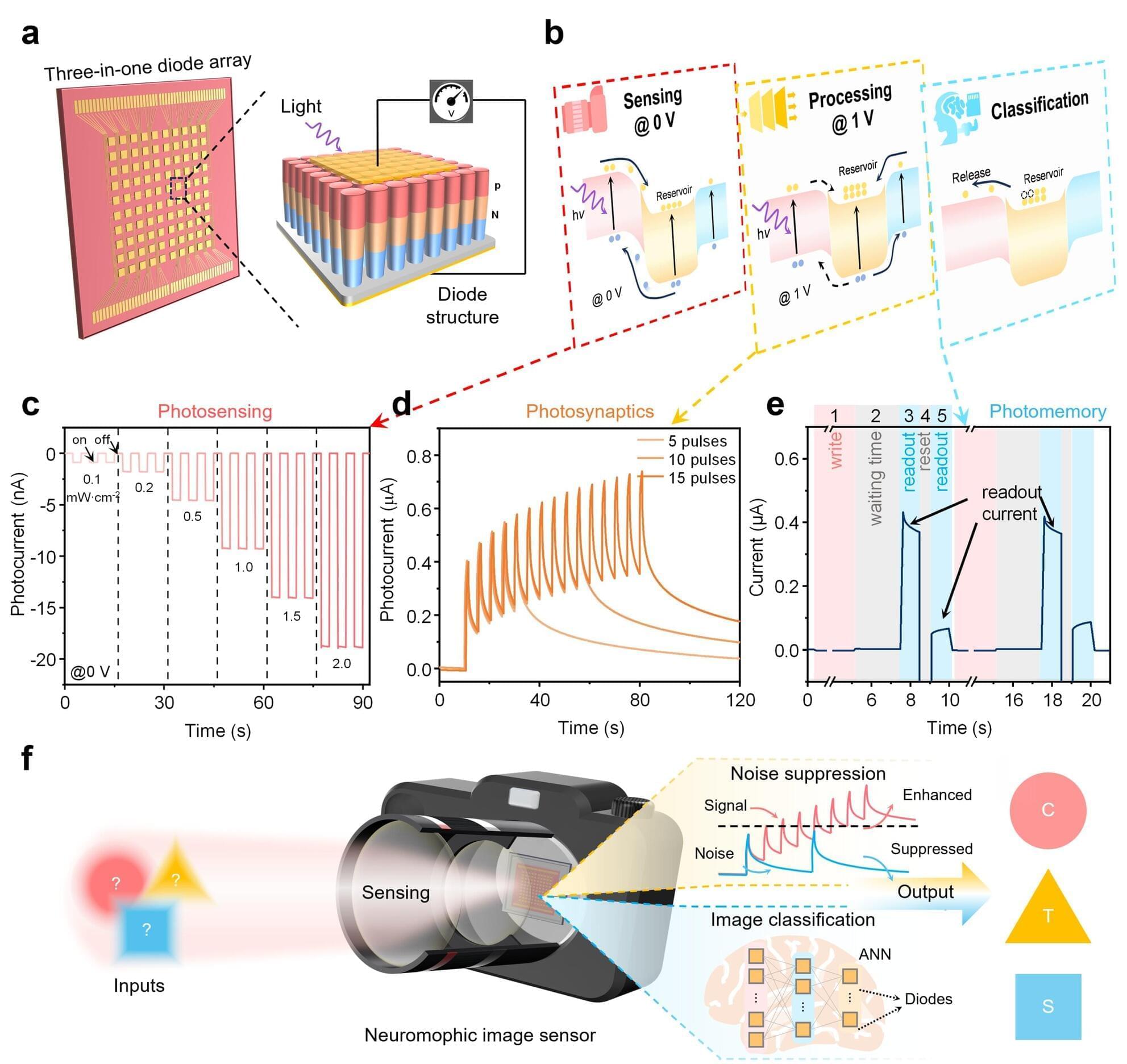
Think about how easily you recognize a friend in a dimly lit room. Your eyes capture light, while your brain filters out background noise, retrieves stored visual information, and processes the image to make a match. It all happens in a fraction of a second and uses remarkably little energy. Unfortunately, artificial vision systems in smartphones, cameras, and autonomous machines operate more like an assembly line. In our recent paper published in Nature Electronics, we describe how we addressed this challenge by enabling sensing, memory, and processing within the same device, pointing to a possible route toward more efficient machine vision.

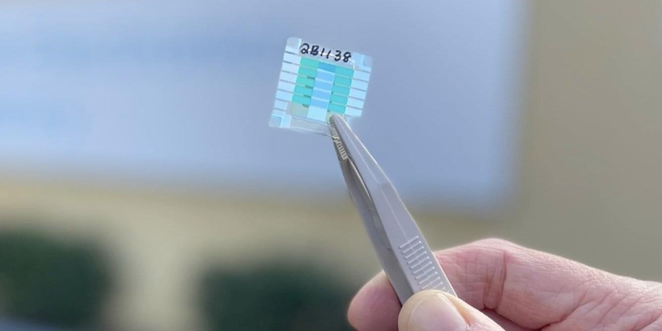
The iGaN Laboratory led by Professor Haiding Sun at the School of Microelectronics, University of Science and Technology of China (USTC), in collaboration with multiple institutions, developed the multifunctional semiconductor diode with integrated photosensing, memory, and processing capabilities.

To understand the challenge, it helps to look at the basic building block of modern digital cameras: the semiconductor p-n diode. These tiny junctions act as the light-sensing pixels in imaging systems. However, a conventional diode is usually limited to a single function. It converts light into an electrical signal, and the captured data must then be transferred to separate memory and processing units. Moving this data back and forth consumes time, power, and chip area.
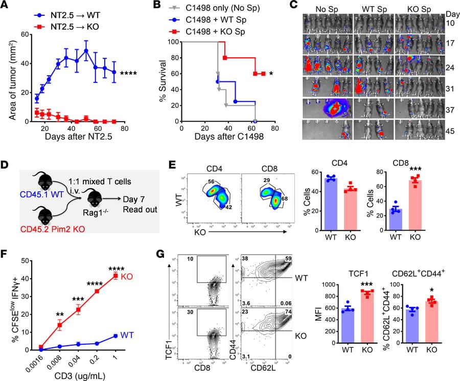
Abstract: The PIM kinase family is involved in tumorigenesis, yet its role in primary T cells remains largely uncharacterized

https://doi.org/10.1172/JCI192928 Here, Xue-Zhong Yu & team identify Pim2 as a key negative regulator of CD8 T-cell antitumor immunity and validate it as a potential therapeutic target for enhancing cancer immunotherapy.

Electron microscopy images show visible autophagosomes in activated WT T cells, but not in Pim2-KO cells, supporting a model in which the PIM2 promotes T cell autophagy.


Address correspondence to: Xue-Zhong Yu or Yongxia Wu, Department of Microbiology and Immunology, Medical College of Wisconsin, 8,701 Watertown Plank Road, Milwaukee, Wisconsin, 53,226, USA. Phone: 414.955.8187; Email: [email protected] (XZY). Phone: 414.955.8148; Email: [email protected] (YW).

Wristband enables wearers to control a robotic hand with their own movements

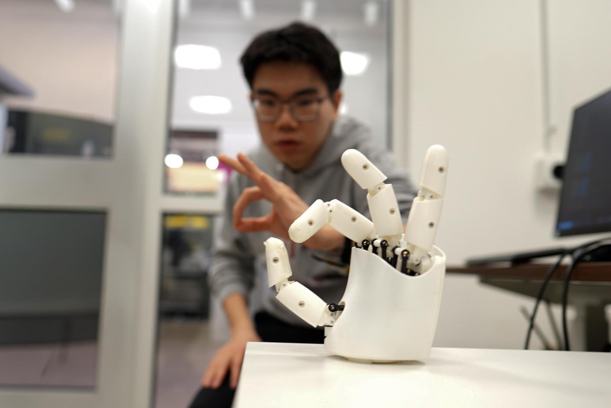
Massachusetts Institute of Technology (MIT) engineers have developed an ultrasound wristband that precisely tracks hand movements in real-time for robotics and virtual reality control.


The next time you’re scrolling your phone, take a moment to appreciate the feat: The seemingly mundane act is possible thanks to the coordination of 34 muscles, 27 joints, and over 100 tendons and ligaments in your hand. Indeed, our hands are the most nimble parts of our bodies. Mimicking their many nuanced gestures has been a longstanding challenge in robotics and virtual reality.

Now, MIT engineers have designed an ultrasound wristband that precisely tracks a wearer’s hand movements in real-time. The wristband produces ultrasound images of the wrist’s muscles, tendons, and ligaments as the hand moves, and is paired with an artificial intelligence algorithm that continuously translates the images into the corresponding positions of the five fingers and palm.

Abstract: ADAMTS7 has been repeatedly associated with coronary artery disease

ADAMTS7 has been repeatedly associated with coronary artery disease.

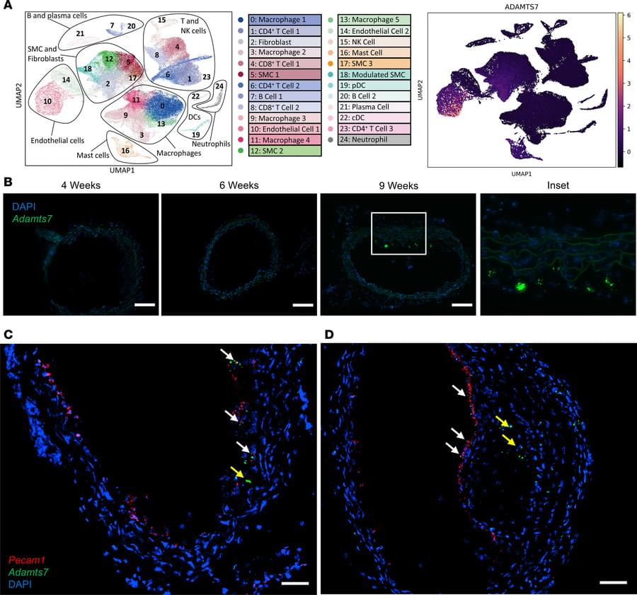
https://doi.org/10.1172/JCI187451 In this Research Article, Robert C. Bauer & team use the largest human atherosclerosis carotid artery scRNA-seq dataset and new mouse models to demonstrate that ADAMTS7 is expressed across multiple vascular cell types and contributes to atherosclerosis by promoting lipid accumulation in smooth muscle cells.

The image shows smooth muscle cells labeled with ZsGreen and counterstained with DAPI (blue) for nuclei—indicating increased foam cells from a diet-induced mouse model of atherosclerosis with Adamts7-overexpressing SMCs were from SMC origin.


1Cardiometabolic Genomics Program, Division of Cardiology, Department of Medicine, Columbia University, New York, New York, USA.

2Department of Biostatistics, Epidemiology and Informatics, University of Pennsylvania Perelman School of Medicine, Philadelphia, Pennsylvania, USA.

Address correspondence to: Robert C. Bauer, Cardiometabolic Genomics Program, Division of Cardiology, Department of Medicine, Columbia University, 630 W. 168th Street, PS10-401, New York, New York 10,032, USA. Phone: 1.212.342.0952; Email: [email protected].

New computational biology for genome sequencing analysis

To improve the ability of metapipeline-DNA to determine where changes in the genome have occurred, the scientists worked with the Genome in a Bottle Consortium led by the U.S. Department of Commerce’s National Institute of Standards and Technology. By incorporating this public-private-academic consortium’s meticulously validated resources, the researchers reduced the rate of false positives without reducing the tool’s precision in finding true genetic variants.

The researchers also produced two case studies demonstrating the pipeline’s capabilities for cancer research. The investigators used metapipeline-DNA to analyze sequencing data from five patients that donated both normal tissue and tumor samples, as well as another five from The Cancer Genome Atlas.

The next step is to get metapipeline-DNA into more labs to accelerate discoveries, and to continue improving the resource with more user feedback. ScienceMission sciencenewshighlights.


In a single experiment, scientists can decipher the entire genomes of many patient samples, animal models or cultured cells. To fully realize the potential to study biology at this unprecedented scale, researchers must be equipped to analyze the titanic troves of data generated by these new methods.

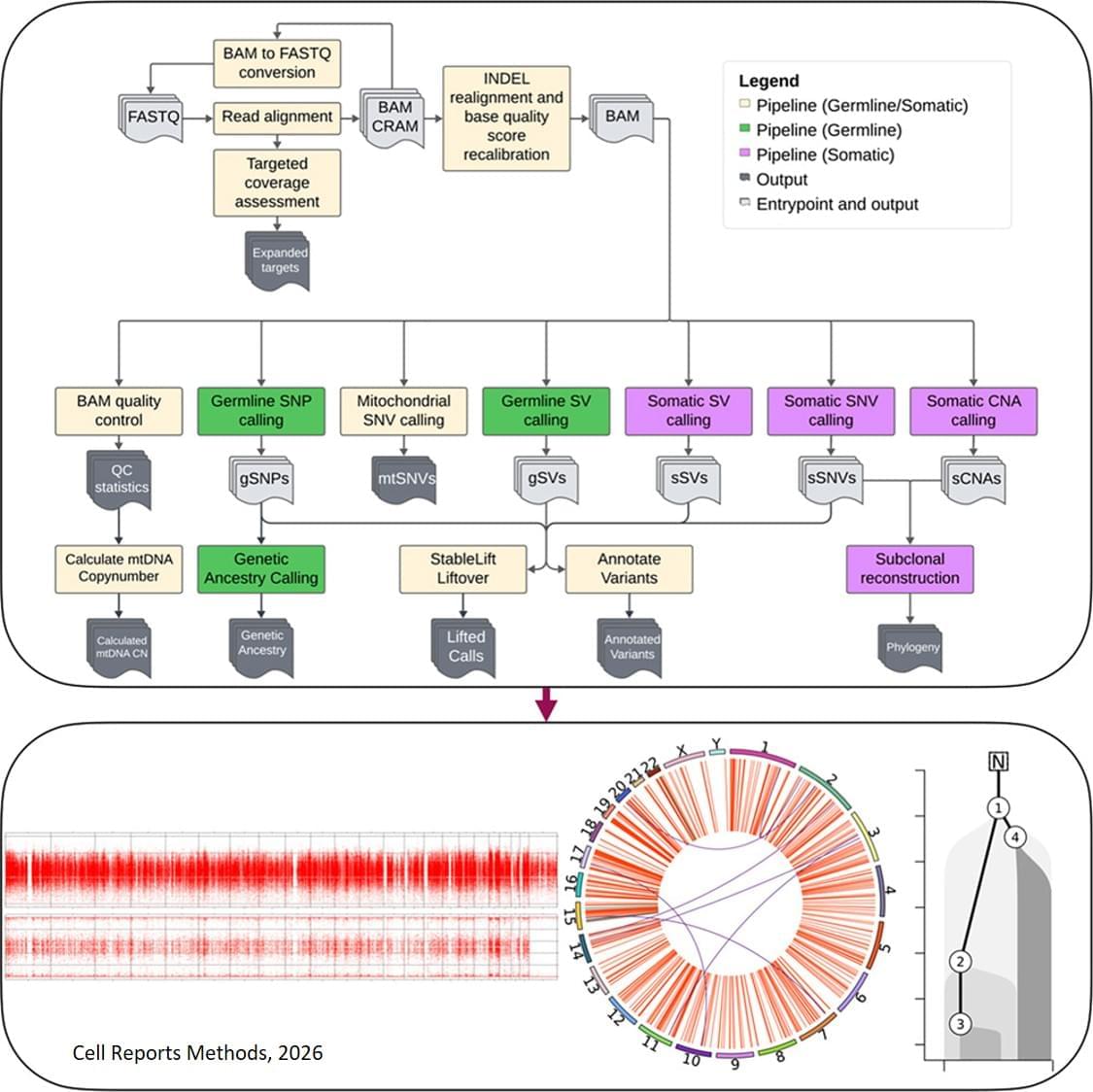
Scientists published findings in Cell Reports Methods discussing building and testing a new computational tool for tackling massive and complex sequencing datasets. The new resource, named metapipeline-DNA, may also make sequencing data analysis more standardized across different research labs.

The sequence of a single human genome represents about 100 gigabytes of raw data, the rough equivalent of 20,000 smartphone photos. The sheer scale of experimental data increases significantly as tens or hundreds of genomes are added into the mix.

Designing better 2D electronics: Addressing anisotropic conductivity to cut contact resistance

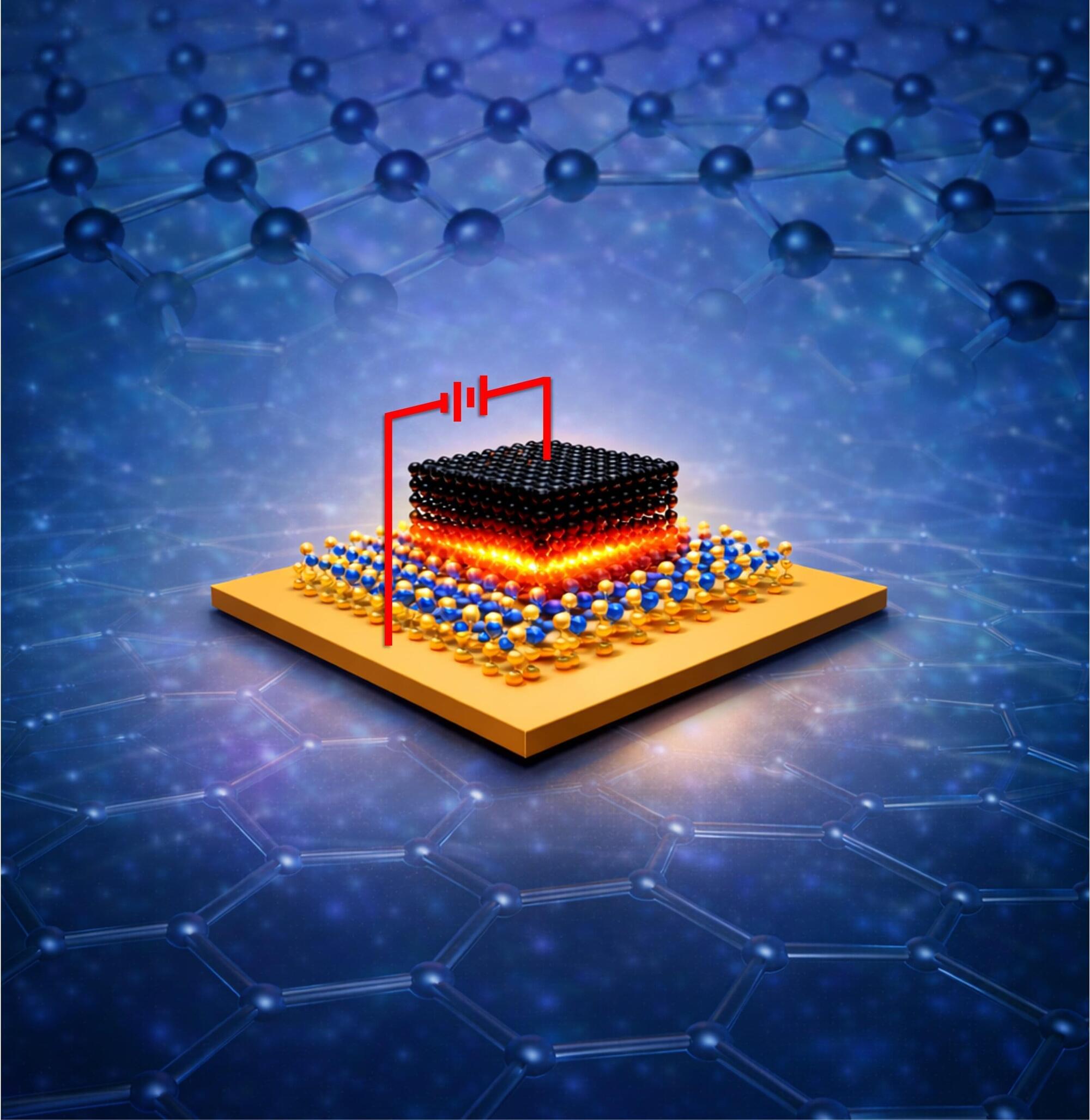
The high-performance semiconductor devices powering smartphone displays, AI computing, EV batteries and more are increasingly incorporating 2D materials to overcome silicon’s scaling limits. To optimize these technologies, a University of Michigan Engineering team developed a precise mathematical framework that accounts for anisotropic—or unevenly spreading—conductivity and device geometry.

Accurate models of how currents move through anisotropic thin films, made of layered 2D materials, can enable the design of more reliable, high-performance nanoelectric devices. Specifically, the model can help engineers reduce current crowding and spreading resistance, essentially current traffic jams, that occur at vertical electrical contacts that connect with the top of a 2D surface. The study is published in ACS Applied Electronic Materials.

New X-ray vision for electronics lets scientists monitor working chips remotely

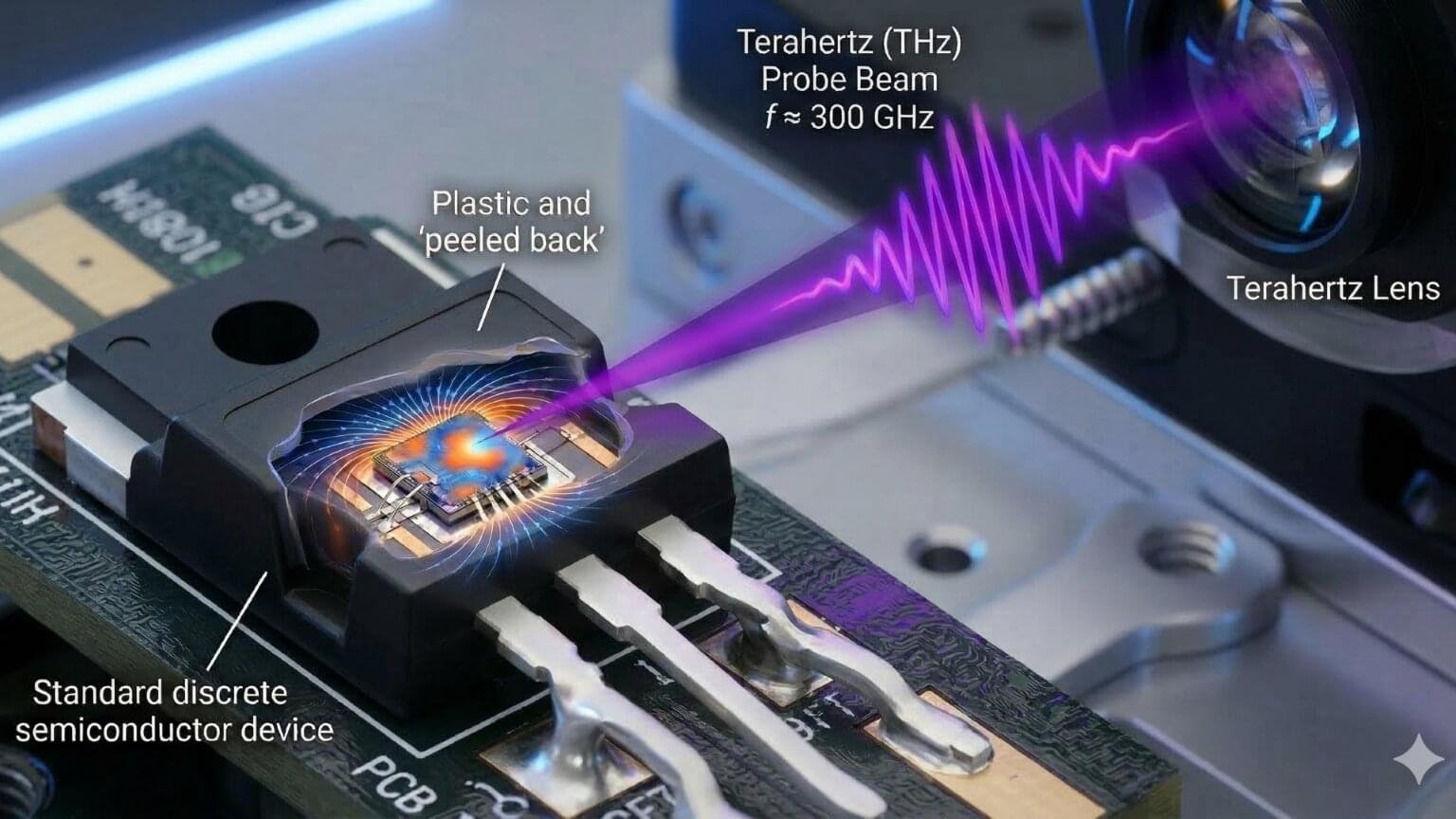
A team of international researchers have developed a breakthrough way to observe what is happening inside electronic chips while they are operating—without touching them, taking them apart, or switching them off. The new technique uses terahertz waves, a safe and non-ionizing form of electromagnetic radiation, to detect tiny movements of electrical charge inside fully packaged semiconductor devices. For the first time, this allows scientists and engineers to monitor electronic components as they function in the real world.

The study, published in the IEEE Journal of Microwaves, involves researchers from Adelaide University in Australia, US technology company Virginia Diodes Inc, the Hasso Plattner Institute and the University of Potsdam, Germany.

Adelaide University Group Leader of the Terahertz Engineering Laboratory (TEL), Professor Withawat Withayachumnankul, said that semiconductors underpin almost every modern technology, from smartphones and medical devices to vehicles, power grids and defense systems.

A world‑first quantum battery charges faster when it gets bigger—but it’s tiny and only lasts nanoseconds

You’re late for an important appointment. Just as you are leaving your house, you realize your phone is flat. Imagine you could charge it almost instantly by exploiting the strange rules of quantum physics. That’s the promise of quantum batteries.

My colleagues and I at CSIRO have developed the world’s first quantum battery prototypes —and the direction the technology has taken is surprising.

/* */